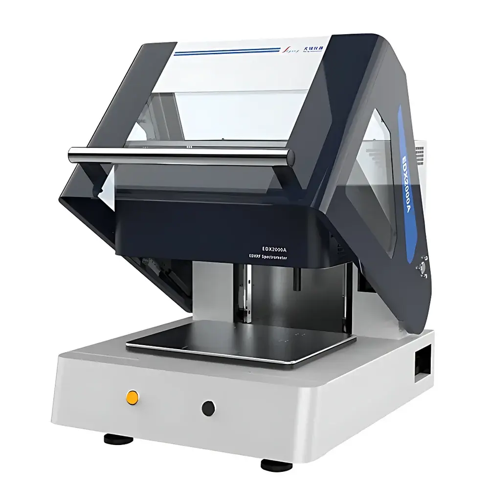
SkyRay EDX 2000A Energy-Dispersive X-Ray Fluorescence (EDXRF) Micro-Area Coating Thickness Analyzer
| Brand | SkyRay Instrument |
|---|---|
| Origin | Jiangsu, China |
| Manufacturer Type | OEM Manufacturer |
| Country of Origin | China |
| Model | EDX 2000A |
| Pricing | Upon Request |
Overview
The SkyRay EDX 2000A is a high-precision, fully automated energy-dispersive X-ray fluorescence (EDXRF) micro-area coating thickness analyzer engineered for non-contact, quantitative measurement of thin metallic and multi-layer coatings on complex geometries. It operates on the fundamental principle of X-ray fluorescence: when a sample is irradiated with high-energy X-rays from a high-power X-ray tube, inner-shell electrons of constituent atoms are ejected; upon electron relaxation, characteristic secondary X-rays are emitted at energies unique to each element. The Fast-SDD (Silicon Drift Detector) captures these emissions with 125 eV energy resolution at Mn Kα, enabling accurate deconvolution of overlapping spectral peaks — critical for resolving multi-layer stacks (e.g., Ni/Cu/Sn on PCB pads or Au/Ni/Cu on semiconductor leads) and heterogeneous substrates (e.g., brass, stainless steel, or ceramic carriers). Unlike conventional benchtop EDXRF systems, the EDX 2000A integrates top-illumination optics, eliminating shadowing effects common in side-irradiation configurations and increasing photon collection efficiency by >2× for low-Z elements and ultra-thin layers (<10 nm).
Key Features
- Top-illumination optical path design optimized for micro-area analysis of irregular surfaces — including concave, convex, threaded, spherical, and stepped geometries — without repositioning or fixture adaptation.
- Motorized XYZ precision stage with sub-micron repeatability (±0.5 µm), programmable trajectory control, and real-time position feedback for automated multi-point mapping across densely packed features (e.g., solder bumps, wafer bond pads, or connector pins).
- Dual-laser alignment system with active Z-height compensation and hardware interlock protection to prevent accidental detector or sample collision during auto-focusing.
- Variable-focus HD optical camera (5–50× digital zoom) synchronized with Z-axis movement and integrated distance correction algorithm — ensures accurate focal plane maintenance over height variations up to ±5 mm, essential for deep recesses, blind vias, and sink-in features.
- High-stability, air-cooled X-ray tube (50 kV / 1 mA max) with optimized anode material and beam collimation for consistent excitation flux and minimized spectral drift over extended operation cycles.
- Onboard spectral calibration verification module with certified reference foils (Cr, Fe, Cu, Zn, Sn, Ag, Au) enabling daily instrument performance validation per ISO 14719 and ASTM B568 compliance protocols.
Sample Compatibility & Compliance
The EDX 2000A accommodates samples ranging from 5 × 5 mm to 300 × 300 mm in footprint and up to 150 mm in height. Its open-stage architecture supports flat wafers, curved automotive trim parts, PCB assemblies, MEMS packages, and jewelry components without custom jigs. The system complies with IEC 61000-6-3 (EMC), IEC 61000-6-4 (emission), and GB/T 18268.1–2010 (industrial EDXRF safety requirements). Software workflows support audit-trail generation, electronic signatures, and data integrity controls aligned with FDA 21 CFR Part 11 and GLP/GMP documentation standards. Measurement uncertainty is traceable to NIST SRM 2136 (Au/Cu/Ni multilayer reference) and certified via annual third-party calibration.
Software & Data Management
SkyRay’s proprietary ThinlinePro™ software provides intuitive, workflow-driven operation: users define measurement points via graphical overlay or coordinate import (CSV/DXF), assign layer models (single/multi-layer, matrix-matched or fundamental parameters), and execute batch runs with auto-reporting. Spectral fitting employs iterative least-squares deconvolution with background subtraction (SNIP algorithm) and matrix correction (Sherman equation-based). All raw spectra, fit parameters, and metadata (date/time, operator ID, stage coordinates, tube settings) are stored in encrypted SQLite databases with immutable timestamps. Export options include PDF reports (with Chinese/English bilingual annotations), CSV for SPC integration, and XML for LIMS interoperability. Built-in QC dashboard monitors detector count rate stability, peak FWHM drift, and calibration check pass/fail status in real time.
Applications
- Semiconductor packaging: Au/Ni/Cu UBM thickness and composition on flip-chip bumps and leadframes.
- PCB manufacturing: ENIG (electroless Ni/immersion Au), ENEPIG, and OSP thickness verification on fine-pitch pads and edge connectors.
- Automotive electronics: Cr/Ni/Cu/Zn trivalent passivation and decorative plating on ABS-plastic grilles and sensor housings.
- Aerospace fasteners: Alodine conversion coating weight (mg/m²) and hexavalent chromium content screening per MIL-DTL-5541.
- Academic research: Quantitative depth profiling of sputtered thin films, diffusion barriers, and nanolaminates using fundamental parameter modeling.
FAQ
What is the minimum detectable thickness for Au on Ni under standard conditions?
For a 30-sec acquisition at 40 kV/0.5 mA, the typical detection limit is ~0.3 nm for Au on Ni (99% confidence, 3σ), assuming homogeneous deposition and no interdiffusion.
Does the system support ISO 3497-compliant plating thickness reporting?
Yes — ThinlinePro™ includes preconfigured report templates compliant with ISO 3497 Annex A (multi-layer EDXRF) and automatically calculates expanded uncertainty (k=2) per GUM guidelines.
Can the EDX 2000A analyze coated wires or cylindrical objects?
Yes — the top-illumination geometry and motorized tilt-adjustable sample holder accommodate cylindrical samples up to Ø80 mm; optional rotation stage enables circumferential averaging.
Is remote diagnostics and firmware update supported?
Yes — secure HTTPS-based remote access allows authorized service engineers to monitor system health, retrieve log files, and deploy validated firmware updates without onsite intervention.
How is spectral interference between Pd and Rh handled in multi-layer analysis?
The 125 eV resolution Fast-SDD enables baseline separation of Pd Lα (2.839 keV) and Rh Lα (2.700 keV); ThinlinePro™ applies constrained peak fitting with physically plausible intensity ratios derived from mass absorption coefficients.


