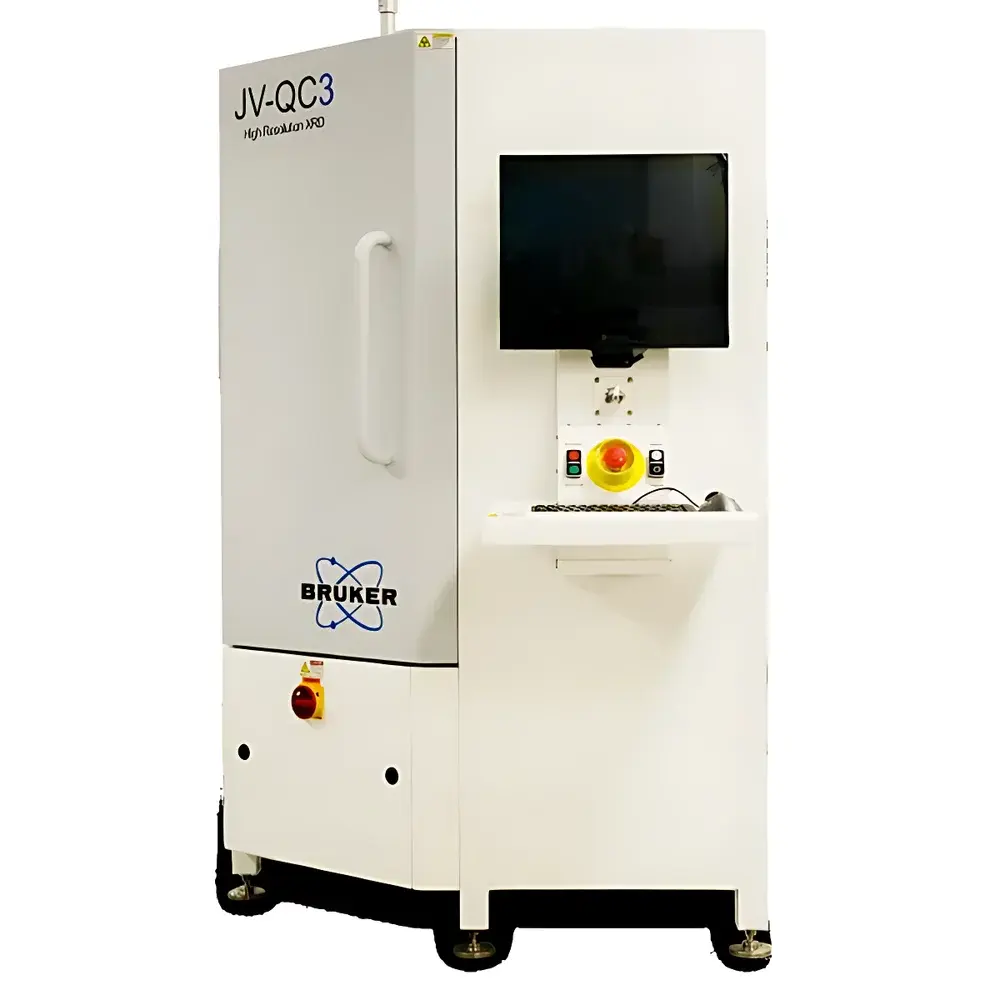
Bruker XRD-JV QC3 High-Resolution Powder X-ray Diffractometer for Semiconductor Process Control
| Brand | Bruker |
|---|---|
| Origin | Germany |
| Instrument Type | Powder X-ray Diffractometer |
| Model | JV QC3 |
| Application Focus | Compound Semiconductor Epitaxial Layer & Substrate QC |
| Automation Level | Fully Automated Wafer Handling (Optional Robotic Arm) |
| Sample Capacity | Up to 4 × 100 mm wafers per batch |
| Compliance | Designed for ISO/IEC 17025-aligned semiconductor manufacturing environments |
| Software Platform | Bruker JV-RADS (Bede RADS) with automated peak fitting, strain/relaxation quantification, and multi-layer compositional analysis |
| X-ray Source Protection | XRG Protect™ tube longevity technology |
| Power Mode | Eco-standby with reduced idle power consumption |
Overview
The Bruker XRD-JV QC3 is a purpose-built, high-resolution powder X-ray diffractometer engineered exclusively for in-line and off-line quality control of compound semiconductor materials in high-volume manufacturing environments. Unlike general-purpose laboratory XRD systems, the JV QC3 implements a fixed-geometry, optimized Bragg-Brentano θ–2θ configuration with high-brilliance Cu Kα or Mo Kα microfocus X-ray source (configurable), monochromated beam path, and high-resolution silicon strip detector—enabling precise lattice parameter determination, epitaxial layer composition quantification, relaxation degree calculation, and strain mapping via reciprocal space mapping (RSM) and omega-2theta scans. Its architecture follows decades of Bruker Semiconductor’s experience in production metrology, succeeding the widely deployed Bede QC200 platform. The system operates on the fundamental principle of constructive interference from crystalline planes satisfying Bragg’s law (nλ = 2d sinθ), with resolution enhanced by angular encoder stability (<0.0001° step resolution), thermal drift compensation, and real-time beam alignment feedback.
Key Features
- Production-grade automation: Optional integrated robotic wafer handler enables unattended loading/unloading of up to four 100 mm wafers (scalable to 150 mm and 200 mm configurations) per sample tray.
- Full workflow automation: Auto-alignment of wafer center and surface normal, automated data acquisition across multiple positions, and real-time intensity normalization using internal reference channels.
- XRG Protect™ technology: Patented X-ray tube thermal management and emission stabilization protocol extends tube lifetime by ≥40% under continuous QC duty cycles.
- Eco-mode operation: Idle power draw reduced to <85 W; full-system warm-up time <15 minutes after standby.
- Dedicated HRXRD optics: Fixed divergence slits, Göbel mirror collimation, and high-efficiency PIXcel3D detector ensure signal-to-noise ratio >250:1 for weak satellite peaks in strained SiGe or AlGaN superlattices.
- Modular geometry support: Configurable goniometer stages enable symmetric, asymmetric, and tilted-symmetric diffraction geometries—including standard ω-2θ scans, rocking curves (ω-scans), and reciprocal space mapping (RSM) for heteroepitaxial systems.
Sample Compatibility & Compliance
The JV QC3 is validated for routine analysis of III–V and II–VI compound semiconductors including GaAs, InP, GaN, AlN, SiC, and sapphire substrates; as well as epitaxial layers such as AlGaN/GaN HEMT stacks, InGaAs/InP quantum wells, and SiGe/Si strained buffers. It supports wafer diameters from 50 mm to 200 mm (with optional stage upgrades), accommodates broken wafers and patterned substrates via programmable stage offset mapping, and integrates barcode scanning for traceable lot tracking. The system meets mechanical and electromagnetic compatibility requirements per EN 61326-1:2013 and is designed to operate within cleanroom Class 1000 (ISO 6) environments. While not certified as a medical device, its measurement protocols align with ASTM F394 (Standard Practice for X-ray Diffraction Analysis of Epitaxial Semiconductor Films) and support GLP/GMP audit readiness through full electronic record retention, user-access logging, and FDA 21 CFR Part 11–compliant software options (available upon request).
Software & Data Management
Control and analysis are executed through Bruker’s JV-RADS software—evolved from the legacy Bede RADS platform—featuring automated peak search, pseudo-Voigt profile fitting, and physics-based modeling of multilayer strain states using dynamical diffraction theory. The software includes built-in templates for common material systems (e.g., GaN-on-sapphire, SiGe-on-Si), supports batch processing of multi-wafer datasets, and exports structured reports in PDF, CSV, and XML formats compliant with SEMI E142 (Data Collection and Exchange Standard). All raw diffractograms, metadata (including goniometer angles, count times, tube current/voltage), and intermediate fit parameters are stored in vendor-neutral HDF5 containers. Remote access is enabled via secure TLS-encrypted HTTP(S) interface, allowing centralized monitoring of tool status, job queueing, and real-time result retrieval without local client installation.
Applications
- Quantitative determination of alloy composition (e.g., InxGa1−xAs, AlxGa1−xN) via lattice parameter shift calibration against Vegard’s law.
- Strain and relaxation analysis of pseudomorphic and relaxed buffer layers using asymmetric (004) or (115) reflections.
- Thickness and interface roughness estimation of thin epitaxial films via X-ray reflectivity (XRR) mode (optional add-on).
- Defect density screening via full-width-at-half-maximum (FWHM) analysis of rocking curves—correlated to threading dislocation density (TDD) per ASTM F2560.
- Process window validation for MBE and MOCVD growth runs, with pass/fail thresholds configurable per product specification.
- Root-cause analysis of wafer bow, slip dislocation generation, or interfacial intermixing through comparative RSM analysis across production lots.
FAQ
Is the JV QC3 suitable for R&D applications, or strictly for production QC?
The JV QC3 is optimized for high-throughput, repeatable metrology—not exploratory phase identification or unknown structure solution. Its fixed-geometry design sacrifices flexibility for speed, precision, and long-term stability required in fab environments.
Can it perform X-ray reflectivity (XRR) measurements?
XRR capability is available as an optional hardware and software module, supporting thickness, density, and interfacial roughness analysis for dielectric and metallic thin films on semiconductor substrates.
What wafer handling options are supported beyond robotic arms?
Manual load ports with vacuum chucks and kinematic alignment pins are standard; cassette-to-chuck auto-loading modules and SMIF pod interfaces are available as factory-installed options.
Does the system support remote diagnostics and predictive maintenance?
Yes—via Bruker’s SecureLink telemetry service (opt-in), which monitors X-ray tube aging, detector gain drift, motor encoder health, and vacuum integrity, triggering service alerts prior to performance degradation.
How is measurement traceability ensured across multiple tools?
Each instrument ships with NIST-traceable Si reference standard; daily automated calibration routines verify angular accuracy to ±0.0005° 2θ, and inter-tool correlation studies are supported through Bruker’s Cross-Tool Validation Package (CTVP).