2D Transition Metal Dichalcogenides (TMDs) Bulk Crystals – MoS₂, MoSe₂, MoTe₂, WS₂, WSe₂, WTe₂ – KEJING High-Purity Single-Crystal Flakes for Exfoliation
| [Brand | KEJING |
|---|---|
| Origin | Hefei, Anhui, China |
| Manufacturer Type | Authorized Distributor |
| Product Category | Research-Grade 2D Material Bulk Crystals |
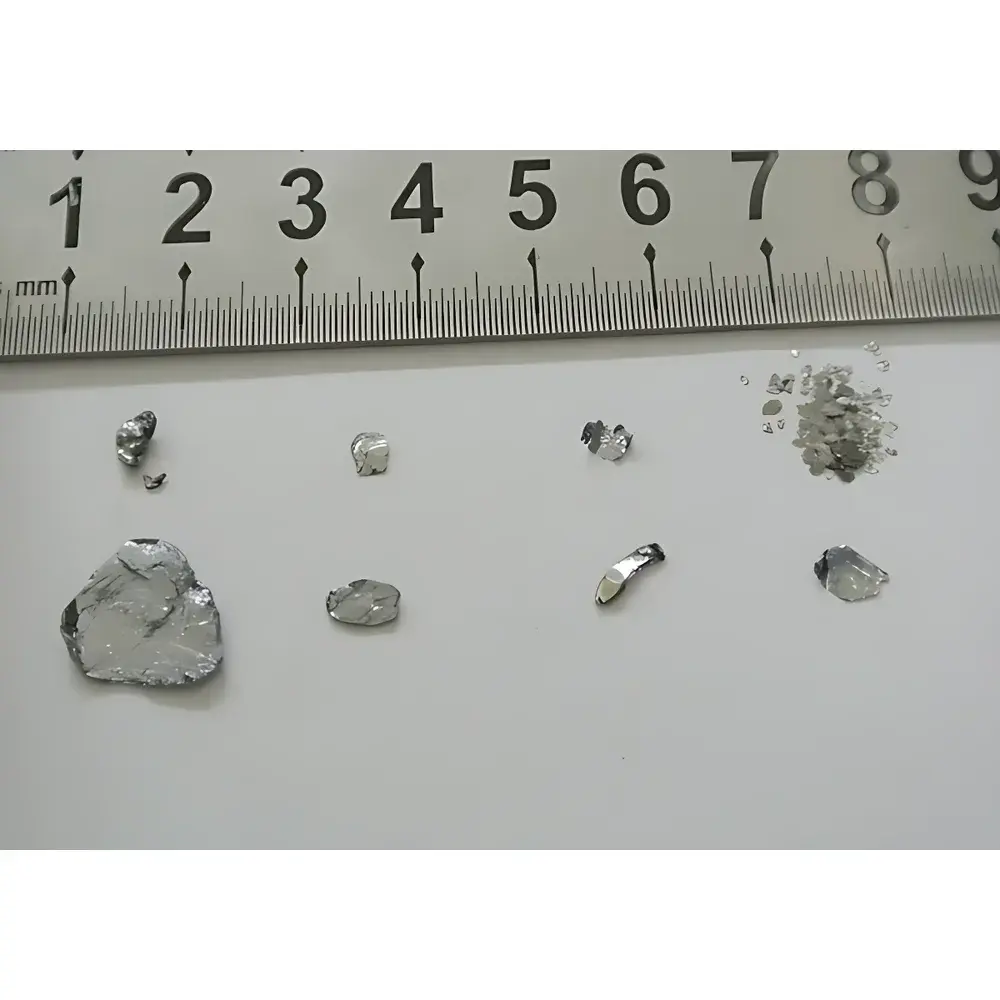
| Dimensions | ~2.0–2.5 mm × 2.0–2.5 mm × ~0.1 mm (typical exfoliation-ready flake) |
| Packaging | Vacuum-sealed in Class 100 cleanroom bags, stored and shipped under inert atmosphere |
| Purity | ≥99.99% (verified by XRD & EDS) |
| Compliance | ISO 9001-certified manufacturing & handling procedures |
| Traceability | Batch-specific QC documentation available upon request] |
Overview
KEJING’s 2D Transition Metal Dichalcogenides (TMDs) bulk crystals are high-purity, single-crystalline starting materials engineered for mechanical or liquid-phase exfoliation into monolayer and few-layer nanosheets. This product line includes six representative TMD compounds—MoS₂, MoSe₂, MoTe₂, WS₂, WSe₂, and WTe₂—each synthesized via chemical vapor transport (CVT) or flux-growth methods to ensure low defect density, high structural homogeneity, and reproducible layer cleavage behavior. These bulk crystals serve as foundational substrates for fundamental research in condensed matter physics, valleytronics, flexible electronics, and heterostructure device fabrication. Unlike polycrystalline powders or CVD-grown films, KEJING’s crystals exhibit long-range atomic order and minimal grain boundary interference, enabling reliable van der Waals stacking and high-mobility transport measurements in transferred devices.
Key Features
- Single-crystalline morphology confirmed by Laue diffraction and polarized optical microscopy
- Controlled stoichiometry and chalcogen vacancy minimization (<0.5% atomic deviation per EDX quantification)
- Consistent cleavage plane (basal 001 orientation) facilitating uniform exfoliation yield (1–3 usable monolayers per flake)
- Available in both natural (MoS₂ only) and synthetic grades—with traceable growth history and post-synthesis annealing records
- Custom sizing options: standard 2.0–2.5 mm square flakes; extended formats (5×5 mm, 10×10 mm, 15×15 mm, 20×20 mm) available for large-area transfer or substrate-assisted growth
- Mass-based procurement option (mg-scale) with linear scalability—ideal for quantitative thin-film deposition calibration or solution-based processing
Sample Compatibility & Compliance
All crystals are handled exclusively in ISO Class 5 (100-level) cleanroom environments and vacuum-packaged in static-dissipative, oxygen/moisture-barrier pouches (H₂O <1 ppm, O₂ <0.1 ppm residual). Each batch undergoes non-destructive surface inspection using white-light interferometry and AFM topography mapping to verify flatness (RMS roughness <0.4 nm over 5×5 µm²). Materials comply with ASTM D7867-22 (Standard Practice for Handling 2D Nanomaterials in Research Laboratories) and support GLP-aligned documentation workflows. Full traceability—including synthesis date, furnace profile log, purification cycle count, and QC test reports—is provided with every shipment. For regulated applications (e.g., NIST-traceable reference standards), custom certification packages meeting ISO/IEC 17025 requirements can be arranged.
Software & Data Management
While the crystals themselves are passive physical standards, KEJING provides complementary digital resources to support experimental reproducibility: a downloadable Material Data Sheet (MDS) containing lattice parameters (a, c), bandgap values (indirect/direct), thermal expansion coefficients, and Raman mode assignments (E²g, A₁g) for each compound; an online batch lookup portal for real-time access to XRD patterns, PL spectra, and HR-TEM micrographs; and integration-ready metadata templates compatible with ELN systems (e.g., LabArchives, Benchling) supporting FAIR data principles (Findable, Accessible, Interoperable, Reusable). All documentation adheres to NIH and ERC open-data guidelines and is version-controlled under SHA-256 checksum verification.
Applications
- Van der Waals heterostructure assembly via dry-transfer or polymer-assisted stamping
- Gate-tunable field-effect transistor (FET) channel fabrication on SiO₂/Si, h-BN, or flexible PET substrates
- Optoelectronic characterization including photoluminescence quantum yield (PLQY), ultrafast carrier dynamics (TRTS, TA spectroscopy), and polarization-resolved reflectance contrast imaging
- Electrocatalytic HER/OER activity benchmarking on carbon paper or Ni foam electrodes
- Scanning probe microscopy (STM/AFM) calibration standards for atomic-resolution tip characterization
- Substrates for epitaxial growth of topological insulators or magnetic 2D layers (e.g., CrI₃, Fe₃GeTe₂)
FAQ
What is the typical exfoliation yield per flake?
Each standard flake (2.0–2.5 mm²) supports 1–3 successful mechanical exfoliations yielding monolayer-to-trilayer flakes suitable for optical identification and device fabrication.
Are these crystals suitable for ultra-high-vacuum (UHV) chamber loading?
Yes—vacuum-baked at 120 °C for 2 hours prior to packaging; outgassing rate <1×10⁻⁹ mbar·L/s·cm² verified by residual gas analysis.
Can I request Raman or XRD validation data for my specific batch?
Absolutely—batch-specific spectral files and peak-fitting reports are included in the digital MDS delivered with each order.
Do you offer wafer-scale TMD crystals?
Not currently; KEJING focuses on research-grade bulk crystals optimized for exfoliation. For wafer-scale epitaxial films, refer to our partner PECVD and sputtering system portfolio.
Is black phosphorus (BP) included in this product line?
Black phosphorus is supplied separately under its own material code (BP-KEJ-001) due to distinct passivation and storage protocols—contact technical support for BP-specific handling guidelines.