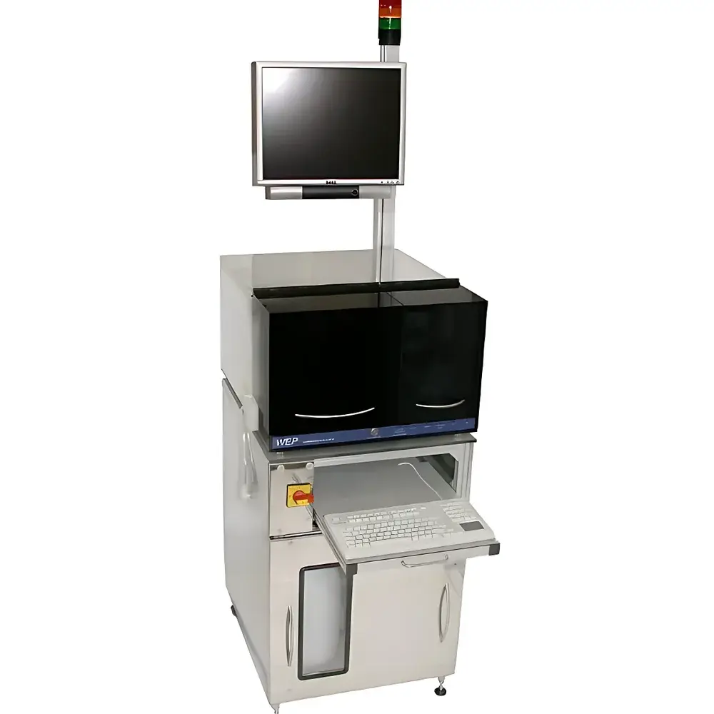
WEP CVP21 Electrochemical Capacitance-Voltage Profiler
| Brand | WEP |
|---|---|
| Origin | Germany |
| Model | CVP21 |
| Measurement Principle | Electrochemical Capacitance–Voltage (ECV) Profiling |
| Carrier Concentration Range | 1×10¹¹ cm⁻³ to 1×10²¹ cm⁻³ |
| Depth Resolution | Down to ≤1 nm |
| Compatible Substrates | Conductive & insulating |
| Wafer Size Support | 4×2 mm² to 200 mm (8″) |
| Material Compatibility | Si, Ge, SiC, GaAs, InP, GaN, AlGaN, InGaN, AlInN, ZnO, CdTe, HgCdTe, and multicomponent III–V/II–VI compounds |
| Automation Level | Fully automated with real-time corrosion monitoring, auto-load/unload, dry-in/dry-out capability |
| Software | Integrated ECV Control Suite with GLP-compliant audit trail, measurement recipe management, and camera-assisted process visualization |
Overview
The WEP CVP21 Electrochemical Capacitance–Voltage Profiler is a precision metrology instrument engineered for quantitative depth-resolved carrier concentration profiling in semiconductor epitaxial layers, diffusion junctions, and ion-implanted structures. It operates on the electrochemical capacitance–voltage (ECV) principle—a solid-state analog of the conventional MOS-CV technique—where controlled anodic dissolution in a tailored electrolyte establishes a moving depletion interface. Capacitance is measured in situ as a function of applied bias, enabling derivation of doping concentration (NA/ND) versus depth via the standard Mott–Schottky relation: 1/C² ∝ Vbi − V − (2ϕF/q), where C is junction capacitance, V is applied voltage, ϕF is Fermi potential, and q is elementary charge. Unlike destructive techniques such as SIMS, ECV provides direct electrical activity quantification without matrix effects or isotopic interference. The CVP21 is widely deployed in R&D labs and pilot lines for compound semiconductor development—including wide-bandgap materials like GaN, SiC, and AlGaN—where precise dopant activation and junction abruptness critically influence device performance in power electronics, RF transistors, and optoelectronic emitters.
Key Features
- Modular cleanroom-compatible architecture with physically isolated optical, electronic, fluidic, and electrochemical subsystems—minimizing cross-talk and enhancing long-term stability.
- High-fidelity capacitance measurement circuitry with sub-femtofarad resolution and integrated automatic cable capacitance compensation—eliminating manual recalibration.
- Real-time color video monitoring of etch front progression via integrated high-magnification camera system; synchronized image capture at each data point enables post-measurement morphological correlation.
- Dry-in/dry-out sample handling with motorized auto-load/unload/reload functionality—supporting wafer-level throughput from 4×2 mm² chips to full 200 mm (8″) wafers without manual intervention.
- Predefined, user-editable measurement recipes with hierarchical access control—enabling lab technicians and process engineers to execute standardized protocols while permitting advanced users to optimize scan parameters (e.g., step size, dwell time, voltage ramp rate).
- Robust electrolyte delivery system with closed-loop flow control, temperature stabilization (±0.1 °C), and chemical compatibility across acidic, basic, and mixed electrolytes for diverse material systems.
Sample Compatibility & Compliance
The CVP21 accommodates electrically active and inactive substrates—including insulating sapphire or SiO₂-on-Si templates—without requiring backside metallization. Its broad material coverage spans elemental (Si, Ge), IV–VI (SiC), III–V (GaAs, InP, GaN), III–N (AlGaN, InGaN), II–VI (ZnO, CdTe), and ternary/quaternary alloys (AlGaAs, AlGaInP, HgCdTe). Each material class requires empirically validated electrolyte formulations (e.g., HF-based for Si, KOH–K₃Fe(CN)₆ for GaN) to ensure stoichiometric dissolution and minimal surface roughening. System operation complies with ISO/IEC 17025 requirements for testing laboratories, and measurement data files include embedded metadata (timestamp, operator ID, instrument serial, calibration status) satisfying FDA 21 CFR Part 11 electronic record integrity criteria. Audit trails are retained for ≥36 months and exportable in CSV/JSON formats for external QA review.
Software & Data Management
The CVP21 runs on WEP’s proprietary ECV Control Suite—a Windows-based application built on .NET Framework with role-based authentication and encrypted local database storage. All measurements generate self-contained project files (.ecvproj) containing raw C–V sweeps, derived N(x) profiles, annotated video frames, and environmental logs (temperature, flow rate, electrode potential). The software supports batch processing of multi-wafer datasets, statistical layer thickness and sheet resistance calculation per ISO 14644-1 cleanroom classification, and export to industry-standard formats (e.g., .csv, .xls, .tdms) for integration with MES or SPC platforms. Optional modules enable GMP-aligned electronic signature workflows, deviation tracking, and periodic system suitability verification reports aligned with ICH Q2(R2) analytical procedure validation guidelines.
Applications
- Quantification of dopant activation efficiency in MOCVD-grown GaN HEMT epiwafers—correlating Mg acceptor concentration with p-type layer conductivity.
- Depth profiling of boron diffusion in silicon after rapid thermal annealing—validating furnace calibration and modeling diffusion coefficients.
- Characterization of graded AlxGa1−xAs heterojunctions for laser diode design—mapping conduction band offset and carrier confinement.
- Verification of selective area doping uniformity across 150 mm SiC MOSFET wafers—supporting CPK analysis for process capability assessment.
- Failure analysis of LED chip leakage paths—identifying unintended dopant pile-up at interface defects via sub-nm depth slicing.
- Development of novel electrolytes for low-damage etching of InGaN quantum wells—using real-time capacitance feedback to halt dissolution at quantum barrier interfaces.
FAQ
What is the minimum measurable carrier concentration with the CVP21?
The system achieves reliable detection down to 1×10¹¹ cm⁻³ in optimized configurations, contingent upon material-specific electrolyte selection and noise-reduction settings.
Can the CVP21 profile insulating substrates such as sapphire or quartz?
Yes—the instrument does not require conductive backside contact; measurement relies solely on the electrochemically formed Schottky-like junction at the electrolyte–semiconductor interface.
Is calibration required between measurements?
No—its fully self-calibrating electronics automatically compensate for parasitic capacitance, eliminating routine user calibration procedures.
How is data integrity ensured for regulated environments?
All measurement sessions generate immutable audit logs with digital signatures, timestamped operator credentials, and hardware fingerprinting—fully compliant with 21 CFR Part 11 and EU Annex 11 requirements.
Does WEP provide application support for non-standard materials?
Yes—customers may submit representative samples for feasibility testing; WEP’s application lab provides method development reports including electrolyte recommendations, voltage sweep parameters, and expected depth resolution estimates.


