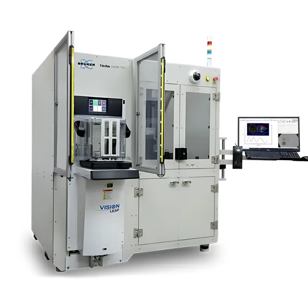
Bruker FilmTek 2000M TSV Reflectance Spectroscopic Metrology System
| Brand | Bruker |
|---|---|
| Origin | USA |
| Model | FilmTek 2000M TSV |
| Optical Configuration | Collimated Beam Reflectometry |
| Spot Size Range | 2 × 1 µm to >100 µm (adjustable via microscope objectives) |
| Spectral Range | 190–1100 nm |
| Spectral Resolution | <1.5 nm FWHM |
| Thickness Measurement Range | 5 nm – 350 µm |
| Compliance | ASTM E2476, ISO/IEC 17025 (when operated in accredited lab environments), supports GLP/GMP data integrity requirements |
Overview
The Bruker FilmTek 2000M TSV is a high-precision, collimated-beam reflectometric metrology system engineered for non-contact, non-destructive thickness and optical constant characterization of single- and multi-layer thin films on planar and patterned substrates. Unlike conventional focused-beam reflectometers—whose high numerical aperture (NA) optics induce angular broadening and incoherent averaging—the FilmTek 2000M employs a patented collimated optical architecture. This design maintains near-normal incidence over the full measurement spot while preserving spectral coherence across wide wavelength ranges (190–1100 nm). As a result, interference fringes in reflected spectra remain well-resolved even for thick dielectric stacks (up to 350 µm), enabling robust modeling of both thin (100 µm) films—including photoresists, SiO₂, SiN, low-k dielectrics, and metal oxides—on silicon, glass, sapphire, and compound semiconductor wafers.
Key Features
- Patented collimated-beam illumination with variable spot size (down to 2 × 1 µm), achieved through interchangeable microscope objectives and precision iris apertures
- High-resolution spectrometer (FWHM <1.5 nm) coupled with real-time CCD imaging for exact spatial registration of measurement location
- Integrated XYZ motorized stage with sub-micron repeatability and programmable mapping capability for wafer-scale uniformity analysis
- Simultaneous acquisition of raw reflectance spectrum and spatial image—enabling traceable correlation between optical response and physical feature geometry
- Optimized for TSV (Through-Silicon Via) metrology: capable of measuring conformal liner/barrier layers inside high-aspect-ratio vias via oblique-angle reflectance mode (optional)
- Modular hardware platform compatible with vacuum and inert-gas purge enclosures for moisture- or oxidation-sensitive films
Sample Compatibility & Compliance
The FilmTek 2000M TSV accommodates rigid planar substrates up to 300 mm diameter and accommodates patterned wafers, reticles, MEMS devices, and advanced packaging substrates (e.g., fan-out wafer-level packages). It supports measurements on opaque and transparent substrates, including Si, GaAs, InP, fused silica, and quartz. The system complies with industry-standard test methodologies referenced in ASTM E2476 (Standard Practice for Spectroscopic Ellipsometry and Reflectometry Measurements on Semiconductor Materials) and aligns with data integrity expectations under FDA 21 CFR Part 11 when deployed with Bruker’s validated software configuration. Audit trails, electronic signatures, and version-controlled model libraries are natively supported for GLP/GMP-regulated environments.
Software & Data Management
Operation is managed through Bruker’s FilmStar™ v6.x software suite, which provides physics-based optical modeling using rigorous transfer-matrix formalism. The software includes built-in dispersion models (Cauchy, Sellmeier, Tauc-Lorentz), multi-layer stack editors, and automated fitting engines utilizing Levenberg-Marquardt and global optimization algorithms. Critical for thick-film analysis, the software computes Power Spectral Density (PSD) transforms directly from measured reflectance data—identifying distinct periodic peaks corresponding to individual layer thicknesses in complex stacks (e.g., SiN/SiO₂ on Si). All raw spectra, fit parameters, PSD outputs, and metadata are stored in vendor-neutral HDF5 format, ensuring long-term archival compliance and third-party interoperability.
Applications
- Front-end-of-line (FEOL) process control: gate oxide, high-k dielectrics, epitaxial layers
- Back-end-of-line (BEOL) monitoring: low-k ILD, Cu barrier/seed layers, CMP endpoint detection
- TSV and 3D integration: liner thickness uniformity in deep vias, conformality assessment of ALD-deposited films
- Advanced packaging: redistribution layer (RDL) dielectric thickness, bump-under-bump metrology
- MEMS and photonics: anti-reflection coatings, Bragg stacks, waveguide cladding layers
- Research & development: rapid screening of novel thin-film materials, optical constant extraction for new deposition processes
FAQ
What distinguishes collimated-beam reflectometry from standard focused-beam systems?
Collimated-beam geometry preserves phase coherence across the entire spectral range by eliminating angular spread at the sample surface—enabling accurate modeling of high-frequency interference oscillations in thick films, which focused systems inherently average out.
Can the FilmTek 2000M measure films on rough or structured surfaces?
Yes—its small-spot collimated beam minimizes scattering artifacts; combined with spatial filtering and PSD-assisted fitting, it delivers reliable results on patterned wafers, trench sidewalls, and moderate surface roughness (Ra < 5 nm).
Is the system qualified for use in ISO Class 5 cleanrooms?
The base platform meets SEMI S2-0215 safety guidelines and can be configured with ESD-safe components, filtered air purge, and vibration-damped optical tables for cleanroom deployment.
How is measurement traceability ensured?
System performance is verified using NIST-traceable reference standards (e.g., Si/SiO₂ step-height wafers); daily calibration routines include spectral response verification and spot-size validation via knife-edge scanning.
Does the software support automated recipe-driven metrology for inline process tools?
Yes—FilmStar™ includes API interfaces (COM/.NET) for integration into factory automation frameworks (SECS/GEM, OPC UA), enabling unattended operation within 24/7 fab environments.


