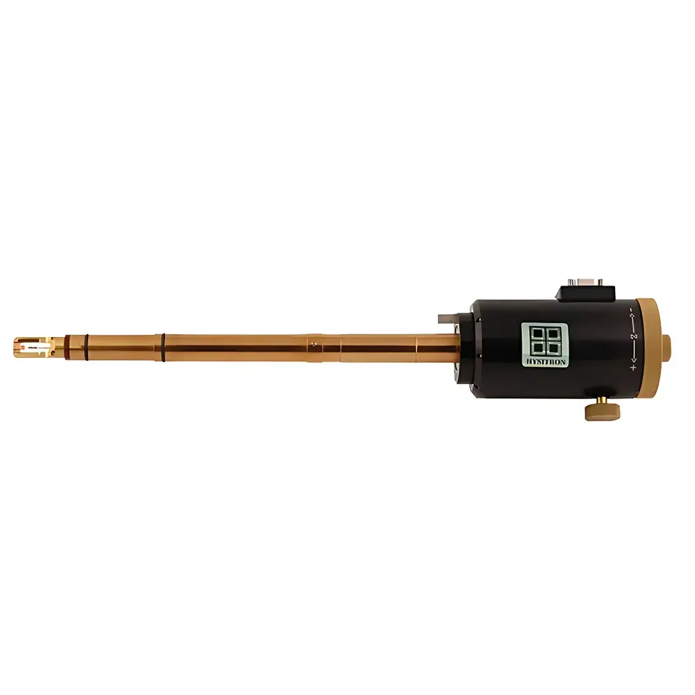
Bruker Hysitron PI 95 In-Situ Nanomechanical Testing System for Transmission Electron Microscopy
| Brand | Bruker |
|---|---|
| Origin | USA |
| Manufacturer Type | Authorized Distributor |
| Origin Category | Imported |
| Model | PI 95 |
| Instrument Type | Integrated Nanoindentation and Scratch Tester |
| Compatibility | JEOL, FEI (Thermo Fisher), Hitachi, Zeiss TEMs (excludes UHR pole-piece configurations) |
| Core Functionality | In-situ TEM-compatible nanomechanical, thermal, and electrical property characterization |
Overview
The Bruker Hysitron PI 95 is a purpose-engineered in-situ nanomechanical testing platform designed exclusively for integration within transmission electron microscopes (TEMs). Leveraging side-entry TEM specimen holders and high-precision piezoelectric actuation, the PI 95 enables real-time, sub-nanometer spatial resolution observation of mechanical deformation processes—such as plasticity initiation, dislocation nucleation, crack propagation, and phase transformation—while simultaneously acquiring quantitative load–displacement data. Its operational principle is grounded in direct-force sensing via integrated capacitive transducers and closed-loop displacement control, ensuring high-fidelity mechanical response measurement under vacuum and high-magnification imaging conditions. Unlike conventional ex-situ nanoindentation, the PI 95 bridges structural evolution and mechanical behavior at true atomic-scale relevance, making it indispensable for fundamental materials science research in metallurgy, semiconductor interfaces, battery electrode degradation, and nanoscale thin-film reliability.
Key Features
- Side-entry TEM-compatible design with standardized 3-mm diameter specimen holder geometry, enabling seamless integration into JEOL, Thermo Fisher (FEI), Hitachi, and Zeiss TEM systems (excluding ultra-high-resolution pole-piece configurations requiring <1 mm clearance)
- Simultaneous multimodal characterization: synchronized acquisition of high-resolution TEM video, load–displacement curves, electrical current–voltage (I–V) traces, and temperature-dependent mechanical response
- Integrated high-sensitivity capacitive force sensor with sub-100 nN resolution and closed-loop displacement control down to 0.02 nm step resolution
- Dual-axis actuation capability supporting uniaxial compression, tension, bending, and lateral scratching modes—all observable in real time at magnifications up to 10⁶×
- Modular architecture allowing field-upgradable functionality: optional high-temperature stage (up to 800 °C), in-situ electro-mechanical coupling module (for piezoresistive or electromigration studies), and nanoscratch attachment with controlled normal load ramping and friction coefficient calculation
Sample Compatibility & Compliance
The PI 95 accommodates standard TEM lamellae prepared by FIB-SEM, electropolished foils, or lift-out specimens with thicknesses between 50 nm and 200 nm. It supports both conductive and insulating samples, with configurable grounding paths and low-noise shielding to minimize electromagnetic interference during concurrent electrical measurements. The system complies with international TEM safety protocols and adheres to ISO/IEC 17025 guidelines for measurement traceability in research environments. All mechanical calibration procedures follow ASTM E2546–22 (Standard Practice for Nanoindentation Testing) and are documented with full audit trails for GLP/GMP-aligned laboratories. No modifications to the host TEM column or vacuum system are required—integration preserves original instrument performance specifications.
Software & Data Management
Control and data acquisition are managed through TriboScan™ v6.x software, a dedicated platform developed by Bruker Hysitron for in-situ TEM experiments. The software provides synchronized timestamp alignment across all data streams—including video frames (via HDMI/SDI input), analog force/displacement channels, thermocouple readings, and digital I/O triggers—enabling frame-accurate correlation between structural events and mechanical thresholds. Raw datasets are stored in HDF5 format with embedded metadata (user, date, TEM parameters, environmental conditions), supporting FAIR (Findable, Accessible, Interoperable, Reusable) data principles. Export options include CSV, MATLAB .mat, and MSA-compatible formats. For regulated environments, optional 21 CFR Part 11 compliance packages are available, including electronic signatures, role-based access control, and immutable audit logs.
Applications
- Real-time observation of dislocation dynamics and stacking fault formation during nanoindentation of single-crystal metals and intermetallics
- In-situ tensile testing of nanowires and 2D material membranes to quantify fracture toughness and strain-to-failure
- Electrochemomechanical degradation analysis of solid-electrolyte interphases (SEI) in Li-ion battery cathodes under bias
- Thermally activated creep and recovery behavior in amorphous alloys and metallic glasses
- Mechanical property mapping across grain boundaries, heterostructures, and phase-separated domains in multilayered thin films
FAQ
Is the PI 95 compatible with aberration-corrected TEMs?
Yes—provided the microscope’s pole-piece gap exceeds 3.5 mm and the side-entry port supports standard Gatan or Oxford Instruments-compatible holder interfaces. UHR configurations with sub-2 mm gaps require custom mechanical adaptation.
Can the system perform quantitative hardness and modulus calculations?
Yes—using Oliver–Pharr methodology applied to synchronized load–displacement curves, with automatic thermal drift correction and contact area function calibration per ISO 14577-1.
What is the maximum achievable strain rate during in-situ tensile testing?
Strain rates range from 10⁻⁴ s⁻¹ (quasi-static) to 10² s⁻¹ (dynamic), depending on specimen geometry and actuator configuration; real-time video capture at ≥100 fps ensures temporal fidelity.
Does the PI 95 support energy-dispersive X-ray spectroscopy (EDS) or electron energy loss spectroscopy (EELS) during testing?
Yes—full compatibility with standard TEM analytical accessories; no signal interference is observed due to RF-shielded cabling and differential grounding schemes.
How is system calibration verified prior to experimental use?
Calibration is performed using NIST-traceable reference standards (e.g., fused silica, sapphire, and SiC), with annual verification recommended per ISO/IEC 17025 requirements.


