Nanonics NSOM Series Scanning Near-Field Optical Microscope
| Brand | Nanonics |
|---|---|
| Origin | Imported (Non-Chinese) |
| Model | NSOM |
| Instrument Type | Materials-Focused SPM Platform |
| Core Function | Scanning Near-Field Optical Microscopy (SNOM/NSOM) with Integrated AFM, Thermal, Electrical, and Raman Capabilities |
| Optical Resolution | ≤50 nm (near-field), 200 nm (confocal), diffraction-limited (far-field) |
| Scan Range | Up to 160 µm (XYZ, dual-probe configuration) |
| Z-Resolution | < 0.02 nm (XY), < 0.05 nm (Z, RMS) |
| Probe Types | Patented glass-fiber probes (metal-coated, hollow, TERS-optimized), compatible with commercial Si cantilevers |
| Feedback | Tuning fork (standard), laser reflection (optional) |
| Detector Compatibility | APD, PMT, InGaAs, CCD, spectrometers |
| Laser Range | Deep UV to NIR |
| Thermal Sensitivity | 0.01 °C |
| Electrical Resolution | < 25 nm (resistive imaging) |
| Max Z-Depth | 140 µm |
| Multi-Probe Support | Up to 4 independently controlled probes |
| Compliance | Designed for GLP/GMP-aligned workflows |
Overview
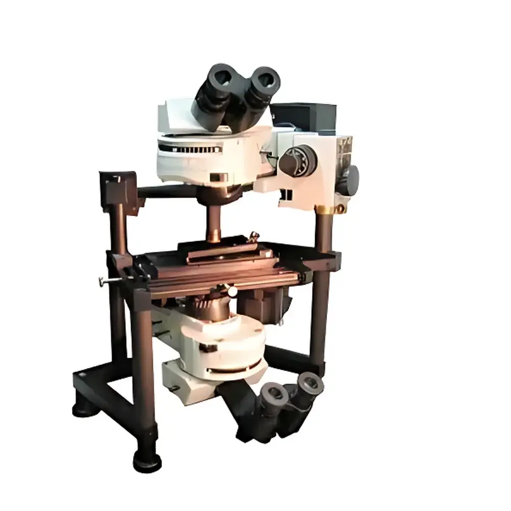
The Nanonics NSOM Series is a high-precision, multi-modal scanning probe microscope engineered for quantitative nanoscale optical, topographic, thermal, electrical, and spectroscopic characterization. Unlike conventional far-field optical microscopes constrained by the Abbe diffraction limit (~200–500 nm), this system implements scanning near-field optical microscopy (SNOM or NSOM) based on evanescent field coupling through sub-wavelength apertures—enabling spatial resolution down to 50 nm. The core measurement principle relies on localized optical excitation and collection via a metal-coated tapered optical fiber probe positioned within ~10 nm of the sample surface. This proximity ensures that only non-propagating near-field components are sampled, decoupling resolution from wavelength. Simultaneously, the platform integrates atomic force microscopy (AFM) functionality—operable in contact, tapping, and non-contact modes—using either sample-scanning or probe-scanning architectures. Its patented dual-stage 3D piezoelectric positioning system (sample scanner: 100 µm XYZ; probe scanner: 30 µm XYZ; combined: up to 160 µm XY) provides exceptional mechanical stability and large-range, high-fidelity nanoscale navigation—critical for correlative multimodal mapping across heterogeneous materials.
Key Features
- Patented glass-fiber NSOM probes with sub-50-nm aperture control, metal coating (Au/Al), and optional hollow-core geometry for nano-pen delivery or TERS enhancement.
- Dual independent scanning architecture: fully decoupled sample and probe motion enables true synchronous multimodal operation without hardware reconfiguration.
- Tuning-fork-based force feedback—immune to optical interference—ensuring robust performance in liquid environments, under laser illumination (e.g., Raman, fluorescence), and during simultaneous optical-electrical-thermal measurements.
- Multi-probe capability: up to four probes operate concurrently and independently—supporting parallel nanomechanical indentation, localized chemical delivery, resistive heating, and optical probing.
- Optically transparent design: open-top and open-bottom optical pathways accommodate upright, inverted, and dual-microscope integration—including confocal, epifluorescence, and 180° backscattering Raman geometries—without compromising AFM/NSOM alignment.
- Z-axis travel of 140 µm enables deep-trench and sidewall profiling inaccessible to standard silicon cantilevers.
- Thermal and electrical probes integrate dual Pt nanowires embedded in insulated glass—delivering <0.01 °C thermal sensitivity and sub-25 nm resistive resolution with minimal contact resistance and long-term oxidation resistance.
Sample Compatibility & Compliance
The NSOM Series accommodates samples ranging from standard 16 mm wafers to oversized substrates up to 200 mm in diameter, including cross-sectional, topographically complex, opaque, and transparent specimens. Its modular stage design permits integration with external SEM, FIB, or optical platforms for hybrid correlative analysis. The system meets engineering requirements for ISO/IEC 17025-compliant laboratories and supports traceable calibration protocols per ASTM E2539 (for AFM) and ISO 18473-3 (for nanoscale optical metrology). When deployed with validated software modules, it satisfies data integrity prerequisites for GLP and GMP environments—including full electronic audit trails, user access controls, and 21 CFR Part 11–compliant signature logging.
Software & Data Management
Acquisition and analysis are managed through Nanonics’ proprietary NanoNavigator™ suite—a modular, scriptable platform supporting real-time synchronization of topography, optical intensity, spectral data (Raman, fluorescence), thermal maps, and current-voltage curves. Raw detector signals (APD, PMT, InGaAs, CCD) are digitized at ≥16-bit resolution with synchronized timestamping. Spectral data streams integrate directly with industry-standard packages (e.g., WiRE, LabSpec) via TCP/IP or HDF5 export. All datasets retain full metadata—including probe type, laser wavelength, feedback gain, environmental conditions—and support batch processing, statistical overlay, and cross-correlation matrix generation. Optional validation packages provide IQ/OQ documentation templates aligned with pharmaceutical and semiconductor QA/QC standards.
Applications
- Nanoscale photonic device characterization: plasmonic nanostructures, waveguide mode profiling, quantum dot emission localization.
- Materials science: strain mapping in epitaxial SiGe layers, domain visualization in ferroelectrics/ferromagnets, carrier diffusion profiling in perovskite solar cells.
- Life sciences: label-free subcellular organelle imaging, membrane protein clustering studies, virus–host interface analysis under physiological conditions.
- Nanofabrication metrology: real-time monitoring of nano-oxidation, laser-assisted etching, and tip-enhanced chemical deposition.
- Failure analysis: buried interconnect inspection in advanced IC packaging, delamination detection at dielectric interfaces, thermal hotspot localization in power devices.
- TERS (Tip-Enhanced Raman Spectroscopy): gold-sphere-functionalized glass probes deliver stable, polarization-tunable enhancement factors >10⁴, enabling single-molecule vibrational fingerprinting on catalytic surfaces.
FAQ
What distinguishes Nanonics NSOM from conventional AFM-coupled optical systems?
Nanonics employs a purpose-built glass-fiber probe architecture—not retrofitted silicon cantilevers—providing broadband optical throughput, polarization fidelity, and mechanical robustness essential for quantitative near-field photonic measurements.
Can the system perform simultaneous NSOM and Raman mapping on opaque samples?
Yes. The open optical architecture supports both top- and bottom-illumination paths, enabling true confocal Raman on bulk metals, ceramics, and thick films without transmission constraints.
Is probe replacement required when switching between thermal, electrical, and optical modes?
No. The multi-probe platform allows dedicated functional probes (e.g., Pt-resistive, Au-TERS, hollow-fiber) to operate concurrently—eliminating downtime associated with manual exchange.
How is nanoscale distance control maintained during NSOM operation?
Topographic feedback is derived from tuning-fork resonance frequency shifts—decoupled from optical interference—ensuring sub-nanometer z-stability even under intense laser illumination or in aqueous media.
Does the system support third-party spectrometers and detectors?
Yes. Standard TTL, analog, and USB interfaces enable seamless integration with Horiba, Renishaw, Andor, and Hamamatsu instrumentation; all synchronization logic is handled internally via NanoNavigator™.


