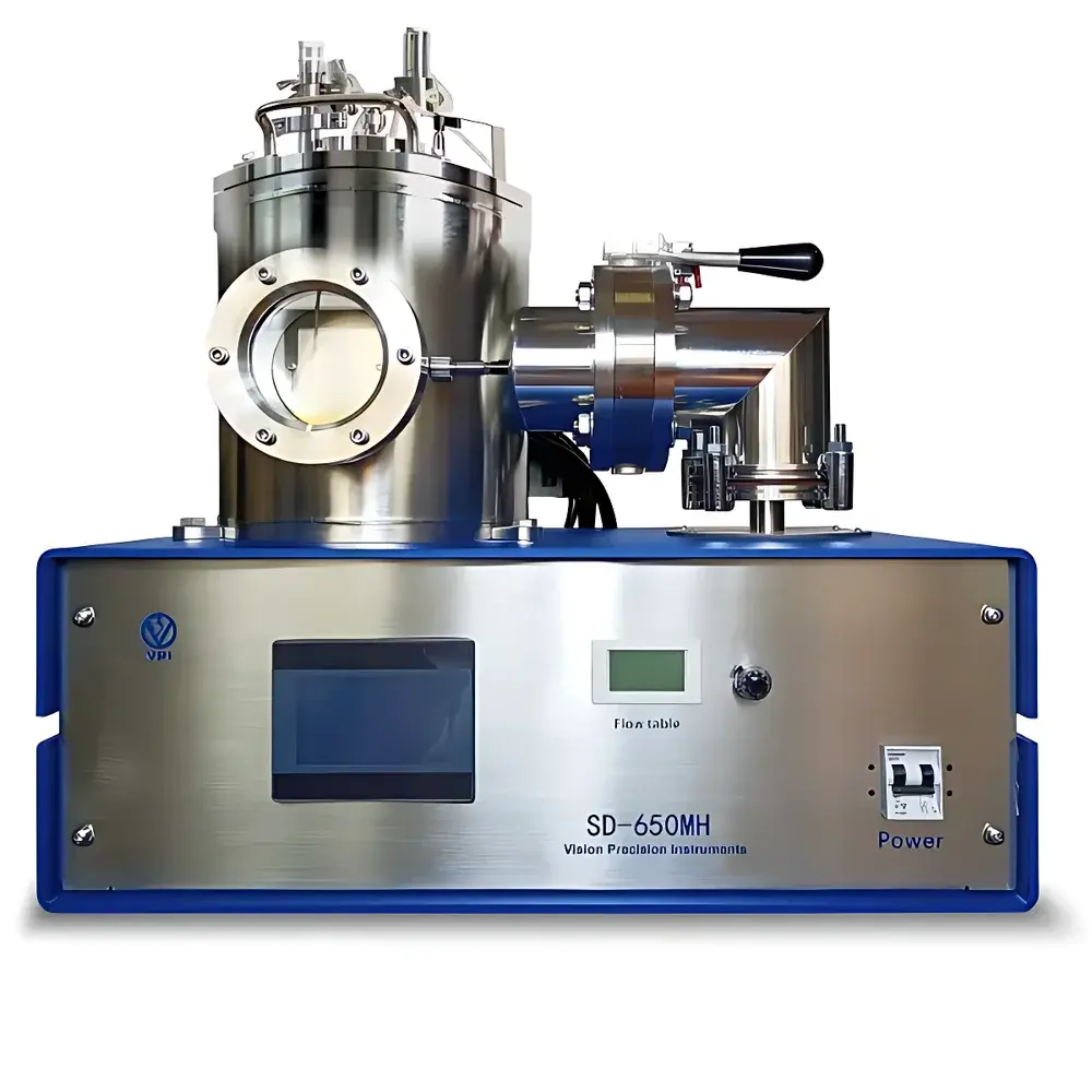
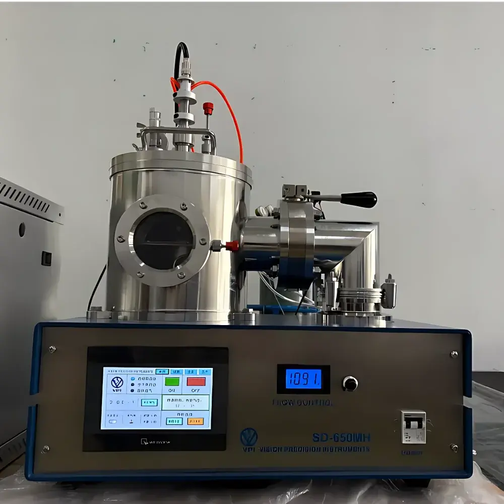
VPI Brooyuan SD-650MHT High-Vacuum Dual-Magnetron Sputtering Coater
| Brand | VPI Brooyuan |
|---|---|
| Origin | Beijing, China |
| Manufacturer Type | Authorized Distributor |
| Country of Origin | Domestic (China) |
| Model | SD-650MHT |
| Target Configuration | Dual Magnetron Sputtering Heads (2× 2-inch) |
| Ultimate Vacuum | ≤5×10⁻⁵ Pa |
| Vacuum System | 300 L/s Turbo Molecular Pump + 4 L/s Scroll Mechanical Pump with Anti-Backstreaming Valve & Oil Filter |
| Vacuum Gauge | Dual-Range Composite Gauge (1×10⁵–1×10⁻⁵ Pa) |
| Power Supply | DC Constant-Current Source (0–600 V / 0–1.6 A), Optional RF Generator (500 W, 13.56 MHz with Auto-Matching Network) |
| Chamber Dimensions (ID) | Ø210 mm × H250 mm |
| Chamber Material | Electropolished 304 Stainless Steel (Ra ≤ 0.8 µm) |
| Substrate Holder | Ø200 mm Rotating Stage (0–20 rpm, ±0.1 rpm precision), Optional Heating (±1 °C) |
| Cooling | Closed-Loop Chiller (±1 °C temperature control) |
| Gas Control | Electromagnetic Mass Flow Valve + Manual Valve (Ar, N₂ compatible) |
| Thickness Monitoring | Integrated Quartz Crystal Monitor (0–6000 nm range, 0.001 nm/s resolution, 257 preloaded materials + user-defined library) |
| Control Interface | VPI-Customized Dual-Touchscreen HMI with Real-Time Parameter Synchronization |
Overview
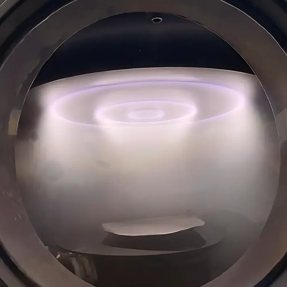
The VPI Brooyuan SD-650MHT is a compact, high-vacuum dual-magnetron sputtering coater engineered for precision thin-film deposition in academic research laboratories and R&D centers. It operates on the principle of magnetron-enhanced physical vapor deposition (PVD), where a crossed electric (E) and magnetic (B) field confines electrons near the target surface, increasing ionization efficiency of argon plasma and enabling high-rate, low-temperature film growth. The E×B drift motion extends electron path length within the plasma confinement zone—typically a closed-loop racetrack above the target—thereby enhancing Ar⁺ ion generation and sustaining stable discharge at pressures as low as 0.1–5 Pa. This configuration delivers superior deposition uniformity, reduced substrate heating (<50 °C rise under typical conditions), and compatibility with conductive, semiconductive, and insulating target materials when paired with optional RF excitation.
Key Features
- Integrated high-rigidity desktop platform (610 × 420 × 220 mm, total height ≤ 720 mm), reducing footprint by 40% versus conventional split-chamber systems while maintaining structural stability against operational vibration.
- Ultra-low-leakage stainless-steel vacuum chamber (304 SS, electropolished interior, Ra ≤ 0.8 µm; leak rate ≤ 5.0×10⁻⁷ Pa·L/s), certified to meet ISO 10110 and ASTM E595 outgassing requirements for ultra-clean thin-film environments.
- Dual independently controllable magnetron heads (2-inch diameter), each equipped with mechanical shutters for pre-sputtering cleaning and sequential or co-deposition capability; optimized magnetic circuit yields ≥800 Gauss surface field strength, improving sputter yield by ~30% over standard designs.
- High-efficiency vacuum train: 300 L/s turbo molecular pump (custom anti-shock design for small-volume chambers) coupled with a 4 L/s scroll-type backing pump featuring triple-stage oil-backstreaming protection (electromagnetic valve, oil mist filter, and one-way check valve).
- VPI-custom dual-touchscreen human-machine interface (HMI) supporting synchronized real-time control of vacuum level, DC/RF power, gas flow (via electromagnetic mass flow valve), substrate rotation speed, and thickness monitoring—fully compliant with GLP audit-trail requirements.
- Substrate stage: Ø200 mm anodized aluminum holder with brushless motor drive (0–20 rpm, ±0.1 rpm repeatability); optional integrated resistive heater (up to 500 °C, ±1 °C stability) for thermally assisted crystallization of oxides and ferroelectrics.
Sample Compatibility & Compliance
The SD-650MHT supports deposition of metallic (e.g., Cu, Al, Ti, NiFe), alloy (NiCr, CoPt), ceramic (Al₂O₃, TiO₂, ZnO), dielectric (SiO₂, Ta₂O₅), ferroelectric (PZT, BTO), and polymer-compatible layers (e.g., PTFE analogs via reactive sputtering). Its modular architecture accommodates substrates up to 150 mm in diameter and thicknesses from 0.1 mm to 10 mm—including silicon wafers, glass slides, flexible polymers, and irregularly shaped samples via custom fixture integration. All wetted components comply with USP Class VI biocompatibility standards; chamber surface finish meets ISO 14644-1 Class 5 cleanroom particulate limits after bake-out. The system satisfies key regulatory prerequisites for materials qualification under ISO/IEC 17025-accredited labs, including traceable calibration records for vacuum gauges (NIST-traceable), power supplies (IEC 61000-4-30), and thickness monitors (ASTM F1591).
Software & Data Management
The embedded VPI Control Suite provides deterministic parameter logging at 100 ms intervals across all subsystems—vacuum pressure, voltage/current waveforms, gas flow rates, rotational speed, and quartz crystal frequency shifts. Data export conforms to HDF5 and CSV formats, with built-in metadata tagging (operator ID, timestamp, recipe name, lot number). Audit trails are time-stamped, immutable, and password-protected per FDA 21 CFR Part 11 Annex 11 guidelines. Remote diagnostics via Ethernet enable secure SSH access for firmware updates and troubleshooting without local intervention. Optional LabVIEW™ and Python SDK support integration into automated material screening workflows (e.g., combinatorial library synthesis).
Applications
- Semiconductor process development: Fabrication of seed layers (Cu, TaN), barrier films, and transparent conductive oxides (ITO, AZO) for MEMS, TFT backplanes, and photovoltaic test structures.
- Functional oxide research: Growth of epitaxial and polycrystalline ferroelectric (Pb(Zr,Ti)O₃), multiferroic (BiFeO₃), and superconducting (YBCO) thin films under controlled oxygen partial pressure (with optional MFC upgrade).
- Surface engineering: Deposition of wear-resistant (TiN, CrN), corrosion-inhibiting (AlCrN), and low-friction (MoS₂, DLC) coatings on biomedical implants and micro-mechanical components.
- Optoelectronic device prototyping: Synthesis of interference-grade optical stacks (MgF₂/Ta₂O₅, SiO₂/TiO₂) and plasmonic nanostructures (Au, Ag) for sensor platforms and metamaterial studies.
- Energy materials: Preparation of solid-state electrolyte interphases (LiPON), cathode overlays (LiCoO₂), and anode current collectors (Cu/Ni bilayers) for next-generation battery cell evaluation.
FAQ
What vacuum level can the SD-650MHT achieve, and how long does pump-down take?
The system reaches ≤5×10⁻⁵ Pa after chamber bake-out (12 h at 120 °C); from atmosphere to 9×10⁻⁴ Pa takes ≤40 minutes under standard conditions.
Can it deposit insulating materials such as Al₂O₃ or SiO₂?
Yes—when equipped with the optional 500 W RF generator and auto-matching network, the system enables stable reactive sputtering of dielectrics using Ar/O₂ or Ar/N₂ mixtures.
Is the rotating substrate stage programmable for multi-step deposition sequences?
Yes—the HMI supports timed stage rotation profiles, synchronized shutter actuation, and power ramping, allowing complex heterostructure fabrication without manual intervention.
Does the system support compliance with GMP/GLP documentation requirements?
All operational parameters are logged with electronic signatures, time stamps, and revision-controlled recipes; full audit trail export is available for regulatory submission.
What maintenance is required for long-term vacuum integrity?
Routine checks include O-ring inspection every 6 months, turbomolecular pump bearing health monitoring (via vibration analysis), and quarterly calibration of the composite vacuum gauge against a reference standard.
Related Products


