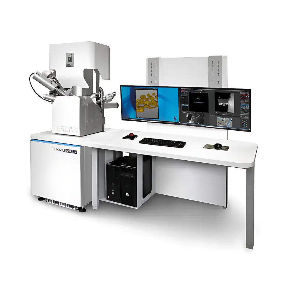
TESCAN SOLARIS Ga⁺ FIB-SEM System with Triglav™ SEM and Orage™ FIB Columns
| Brand | TESCAN |
|---|---|
| Origin | Czech Republic |
| Manufacturer | TESCAN ORSAY HOLDING a.s. |
| Type | Imported High-Resolution Dual-Beam FIB-SEM |
| Model | TESCAN SOLARIS |
| Price Range | USD 1.3–2.0 million (FOB Europe) |
Overview
The TESCAN SOLARIS is a next-generation dual-beam focused ion beam–scanning electron microscope (Ga⁺ FIB-SEM) engineered for nanoscale imaging, precision sample preparation, and correlative 3D microstructural analysis. It integrates two purpose-built, high-performance columns: the Triglav™ field-emission SEM column—optimized for ultra-high-resolution imaging at low accelerating voltages—and the Orage™ liquid metal ion source (LMIS) FIB column—designed for sub-20 nm TEM lamella preparation, high-fidelity nanomachining, and large-volume serial sectioning. Unlike legacy platforms, the SOLARIS architecture enables simultaneous acquisition of secondary electrons (SE), backscattered electrons (BSE), energy-filtered BSE, EDS, and EBSD signals during FIB milling or SEM imaging—facilitating true in situ multimodal characterization. Its core measurement principle relies on coordinated scanning of a finely focused gallium ion beam (for sputtering, deposition, and cross-sectioning) and a high-brightness Schottky field-emission electron beam (for high-contrast, surface-sensitive imaging), both operating under ultra-stable vacuum conditions (<1×10⁻⁷ mbar in the specimen chamber).
Key Features
- Triglav™ SEM Column: Delivers <1.0 nm resolution at 1 kV and <0.6 nm at 30 kV; incorporates an in-column multi-detector system with energy filtering capability to selectively acquire low-loss BSE for enhanced surface sensitivity and material contrast.
- Orage™ FIB Column: Features advanced ion optics enabling <5 nm resolution at 500 eV landing energy; supports continuous ion beam current from 1 pA to 100 nA—enabling both atomic-scale polishing and rapid bulk removal.
- Essence™ Software Platform: Modular, workflow-driven interface with automated lamella preparation protocols, customizable dashboard layouts, and integrated scripting (Python API) for reproducible, GLP-compliant operation.
- OptiGIS™ Gas Injection System: Up to six independently controllable OptiGIS units; optional coaxial 5-nozzle configuration for simultaneous precursor delivery (e.g., Pt, W, C, SiO₂, XeF₂) during milling or deposition.
- In Situ Analytical Capabilities: Real-time EDS mapping and EBSD pattern acquisition synchronized with FIB slicing—enabling 3D crystallographic reconstruction and compositional tomography without stage repositioning.
- Adaptive Beam Optimization: Auto-tuned probe formation across beam currents; piezo-driven aperture changer and stabilized high-voltage supply ensure repeatability in beam alignment and spot size control.
Sample Compatibility & Compliance
The TESCAN SOLARIS accommodates standard 3” (75 mm) and 4” (100 mm) wafers, TEM grids (3 mm), and irregularly shaped specimens up to 150 mm in diameter and 50 mm in height. Its charge compensation module—including low-energy electron flood gun and adjustable bias electrode—enables stable imaging and milling of non-conductive materials (e.g., ceramics, polymers, biological tissue) without conductive coating. The system complies with IEC 61000-6-2/6-4 (EMC), CE Machinery Directive 2006/42/EC, and ISO 14644-1 Class 5 cleanroom requirements for installation. All software logging—including instrument parameters, user actions, and acquisition metadata—supports audit trails compliant with FDA 21 CFR Part 11 and ISO/IEC 17025 for accredited laboratories.
Software & Data Management
Essence™ provides native support for FAIR data principles: raw images, spectra, and stage coordinates are stored in open HDF5 format with embedded metadata (MIAME/MINSEQ-compliant). Batch processing pipelines include automated drift correction, slice-to-slice registration, and EDS quantification using Cliff-Lorimer or ZAF methods. For 3D reconstruction, the bundled TESCAN Microstructure Reconstruction Suite (MRS) performs iterative alignment, segmentation (AI-assisted U-Net models), and mesh generation compatible with Avizo, Amira, and Paraview. Data export options include TIFF (16-bit), CSV (spectrum), and CTF (crystallographic orientation maps). Remote monitoring and secure access are enabled via TLS-encrypted web interface supporting SAML 2.0 authentication.
Applications
- Transmission Electron Microscopy (TEM) Sample Preparation: Automated lift-out and final polishing at ≤500 eV to produce electron-transparent lamellae <20 nm thick with minimal amorphous layer and ion damage.
- 3D Nanotomography: Serial sectioning at 5–50 nm slice thickness with concurrent EDS/EBSD acquisition for quantitative phase distribution and grain boundary network analysis in alloys, battery cathodes, and geological samples.
- Nanofabrication & Circuit Edit: Precise IC deprocessing, via drilling, and maskless lithography using ion-induced deposition (Pt, W) or etching (XeF₂).
- Life Sciences: Cryo-FIB-SEM workflows (with optional cryo-transfer system) for vitrified cellular ultrastructure imaging and targeted lamella extraction.
- Materials Failure Analysis: Cross-sectional analysis of delamination, voids, and interfacial reactions in multilayer thin-film devices and additive-manufactured components.
FAQ
What is the minimum achievable lamella thickness using the SOLARIS for TEM preparation?
Typical final lamellae range from 15–25 nm in thickness, depending on material hardness and final polishing voltage (down to 500 eV); amorphous layer thickness is typically <2 nm for Si and <5 nm for Cu.
Does the system support automated EBSD indexing during FIB milling?
Yes—EBSD patterns are acquired in real time during slicing using the integrated Hikari Super camera and OIM Analysis™ software; indexing rates exceed 95% at 10 kV and ≥500 fps frame rate.
Can the Essence™ software be validated for GxP environments?
Yes—full IQ/OQ/PQ documentation packages are available; software includes electronic signatures, role-based access control, and immutable audit logs meeting FDA 21 CFR Part 11 and EU Annex 11 requirements.
Is the Orage™ FIB column compatible with alternative ion sources?
No—the Orage™ column is optimized exclusively for Ga⁺ LMIS; however, TESCAN offers separate Xe plasma FIB (PFIB) systems (e.g., TESCAN AMBER) for higher throughput applications.
What vacuum level is maintained in the sample chamber during EBSD acquisition?
The chamber operates at ≤2×10⁻⁶ Pa during EBSD to minimize electron scattering and ensure high pattern quality; differential pumping isolates the FIB column to maintain <1×10⁻⁸ Pa at the ion source.


