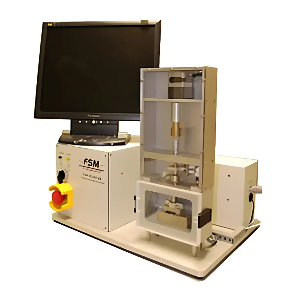
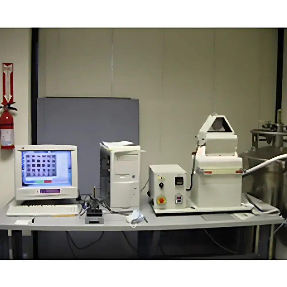
FSM Film Adhesion Tester Model FA-2000
| Brand | FSM |
|---|---|
| Origin | USA |
| Manufacturer Type | Authorized Distributor |
| Origin Category | Imported |
| Model | FA-2000 |
| Pricing | Available Upon Request |
Overview
The FSM FA-2000 Film Adhesion Tester is an engineered metrology system designed for quantitative evaluation of interfacial adhesion strength between thin films, multilayer stacks, and rigid substrates—primarily silicon wafers, glass, sapphire, and ceramic carriers used in semiconductor front-end-of-line (FEOL) processes, 3D IC integration (e.g., TSV and BWS), and advanced packaging. It operates on the principle of controlled mechanical delamination using standardized probe-based indentation or scratch methodologies compliant with ASTM D3359 (cross-hatch), ISO 2409, and modified versions of ASTM C1624 (scratch adhesion testing). Unlike qualitative visual assessment tools, the FA-2000 delivers repeatable, load-calibrated force-displacement data to determine critical adhesion thresholds—including onset of cohesive failure, interfacial debonding, and propagation energy—enabling correlation with process parameters such as deposition temperature, plasma treatment, annealing cycles, and interfacial chemistry.
Key Features
- Two calibrated adhesion test modes: low-strength (< 5 MPa) micro-scratch and medium-strength (5–80 MPa) controlled-indentation delamination, each with traceable NIST-traceable load cell calibration (±0.5% full scale)
- Integrated high-resolution optical imaging (5 MP CMOS, 0.5 µm/pixel) synchronized with real-time force feedback for precise failure mode classification (adhesive vs. cohesive vs. mixed-mode)
- Automated stage with ±0.1 µm positional repeatability and programmable scan paths for spatial mapping across 200 mm and 300 mm wafers
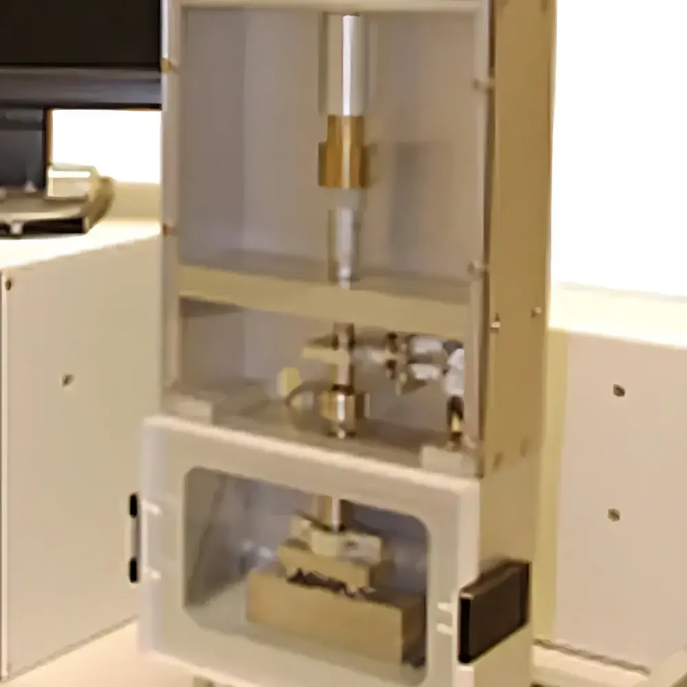
- Modular probe interface supporting interchangeable diamond-tipped, spherical, and conical indenters (tip radii: 1 µm to 50 µm) and custom scratch stylus geometries
- Ruggedized vacuum-compatible chamber design for in situ testing under inert or controlled ambient conditions (optional N₂ purge or low-humidity operation)
- Compliance-ready firmware with audit trail logging, user access levels (admin/operator), and timestamped test records aligned with GLP/GMP documentation requirements
Sample Compatibility & Compliance
The FA-2000 accommodates planar substrates up to 300 mm in diameter and thicknesses ranging from 50 µm to 2 mm, including ultra-thin wafers (UTW), SOI, compound semiconductors (GaAs, SiC), and optoelectronic substrates. It supports single-layer films (e.g., SiO₂, SiNₓ, TiN, Al, Cu) and complex stacks (e.g., BEOL metal/dielectric stacks, passivation layers, MEMS structural films). All test protocols adhere to industry-accepted standards: ASTM D3359 (tape test for qualitative screening), ISO 2409 (equivalent cross-hatch method), and ASTM C1624 (quantitative scratch adhesion classification). Data output formats comply with SEMI E142 (data exchange for wafer-level metrology) and support integration into factory MES systems via SECS/GEM protocol.
Software & Data Management
The FSM AdhesionSuite v4.2 software provides full instrument control, real-time visualization of load-displacement curves, and automated failure event detection using derivative-based threshold algorithms. Each test generates a structured XML report containing raw sensor data, image metadata, environmental logs (temperature, humidity), operator ID, and calibration certificate references. The system supports 21 CFR Part 11-compliant electronic signatures, role-based permissions, and encrypted local database storage with optional cloud backup (AWS S3 or on-premise NAS). Export options include CSV, PDF (with embedded images and statistical summaries), and HDF5 for machine learning pipeline ingestion.
Applications
- FEOL process development: quantifying impact of PECVD parameters on SiNₓ/SiO₂ adhesion to silicon
- TSV barrier/seed layer qualification: evaluating Ta/TaN/Cu stack integrity after electrochemical deposition and annealing
- Wafer-level packaging: assessing dielectric adhesion in redistribution layers (RDLs) and under-bump metallization (UBM)
- MEMS reliability: monitoring time-dependent interfacial degradation under thermal cycling or humidity exposure
- Failure analysis labs: root-cause identification of blistering, edge lift-off, or crater formation in production wafers
- Materials R&D: benchmarking novel low-k dielectrics, atomic-layer-deposited (ALD) oxides, and hybrid organic-inorganic films
FAQ
What film thickness ranges can the FA-2000 accurately characterize?
The system is optimized for films between 10 nm and 5 µm thick; sub-10 nm layers require complementary techniques (e.g., XRR or nanoindentation) due to signal-to-noise limitations in mechanical delamination.
Does the FA-2000 support automated lot-level reporting for high-volume manufacturing?
Yes—AdhesionSuite includes batch processing workflows, statistical process control (SPC) charting (X-bar/R, Cp/Cpk), and configurable pass/fail criteria per site or layer stack.
Is calibration verification required before each test run?
No—daily verification using certified reference samples (FSM-REF-ADH-01) is recommended; full recalibration is performed annually or after major maintenance per ISO/IEC 17025 guidelines.
Can the system be integrated into a cleanroom environment?
Yes—the FA-2000 meets SEMI S2/S8 safety standards and features ESD-safe construction, Class 100-compatible enclosure options, and vibration-isolated optical table mounting kits.


