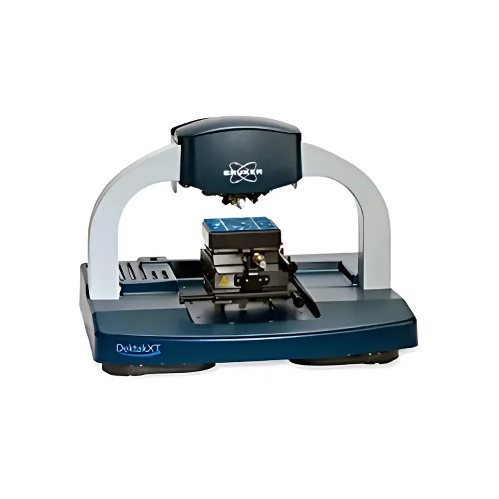
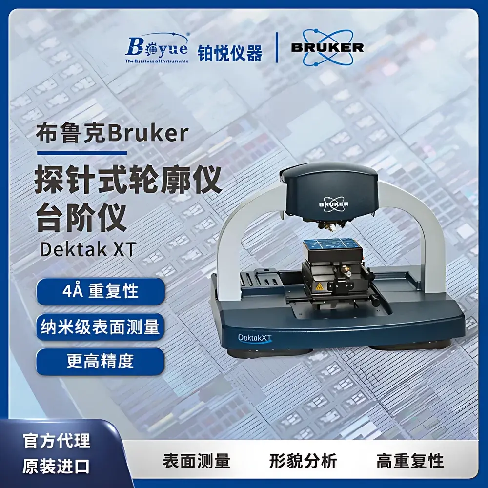
Bruker Dektak XT Stylus Profilometer for Nanoscale Surface Topography Measurement
| Brand | Bruker |
|---|---|
| Origin | Germany |
| Manufacturer Type | Authorized Distributor |
| Product Category | Imported Instrument |
| Model | Dektak XT |
| Price Range | USD 55,000–68,000 (FOB Hamburg) |
| Vertical Measurement Repeatability | <5 Å |
| Vertical Resolution | 1 Å |
| Accuracy | ±1% of measured step height |
| Tip Radius | 50 nm – 25 µm |
| Normal Force Range | 0.3–15 mg (adjustable in 0.1 mg increments) |
| Maximum Scan Length | 55 mm (2-inch stage travel) |
| Maximum Sample Diameter | 50 mm |
| Vertical Measurement Range | Up to 1 mm |
Overview
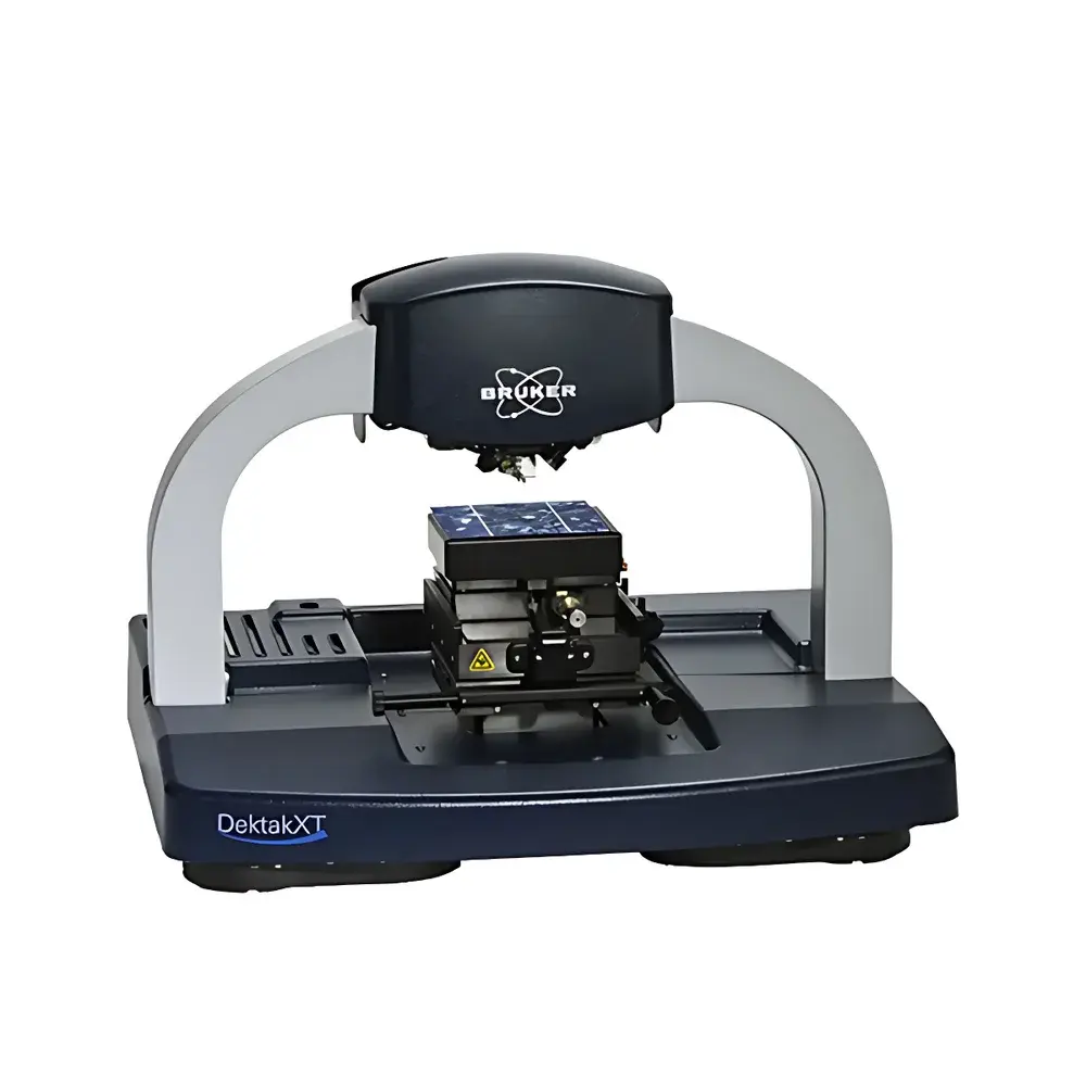
The Bruker Dektak XT is a high-precision, motorized stylus profilometer engineered for nanoscale surface topography characterization across research and production environments. Operating on the principle of mechanical contact profilometry—where a diamond-tipped probe traverses the sample surface while a linear variable differential transformer (LVDT) transduces vertical displacement—the Dektak XT delivers traceable, quantitative measurements of step height, roughness, curvature, and film thickness with sub-angstrom vertical resolution. Its closed-loop Z-axis feedback architecture ensures exceptional linearity and long-term stability, making it suitable for applications demanding metrological rigor, including semiconductor process control, photovoltaic metallization verification, MEMS device qualification, and microfluidic channel depth profiling. Designed and manufactured in Germany, the instrument complies with ISO/IEC 17025-relevant calibration traceability frameworks and supports GLP/GMP-aligned workflows through audit-trail-capable software.
Key Features
- Sub-angstrom vertical resolution (1 Å) enabled by low-noise analog signal conditioning and high-stability LVDT sensing
- Programmable normal force control (0.3–15 mg) with NLite+ low-force mode for delicate photoresists, polymer films, and soft biomaterials
- Motorized 55 mm scan range with auto-focus and multi-point leveling for consistent tip-sample engagement across non-planar substrates
- Interchangeable diamond tips (50 nm–25 µm radius) optimized for varying surface geometries—from sharp lithographic steps to broad curvature profiles
- Integrated vibration isolation platform and temperature-compensated granite base for measurement stability in standard lab environments
- Compliance-ready firmware supporting 21 CFR Part 11 electronic signatures, user access levels, and full audit trail logging
Sample Compatibility & Compliance
The Dektak XT accommodates wafers, glass slides, metal foils, and polymer substrates up to 50 mm in diameter and 25 mm in thickness. Its non-destructive, low-force scanning enables repeatable characterization of photosensitive layers (e.g., SU-8, AZ series), thin-film solar cell electrodes (Ag gridlines), and MEMS structural layers without inducing plastic deformation or tip wear artifacts. The system meets ASTM E1094 (Standard Test Method for Measuring Step Height Using a Mechanical Profilometer) and aligns with ISO 25178-2 (Geometrical Product Specifications — Surface Texture) for areal roughness reporting. Calibration is performed using NIST-traceable step height standards (e.g., 100 nm, 1 µm, 10 µm SiO₂-on-Si reference wafers), with certificate documentation available per IEC 61000-4-3 EMC and CE marking requirements.
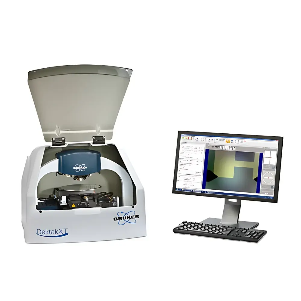
Software & Data Management
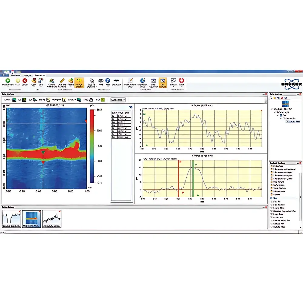
Vision64 software provides a validated, Windows-based interface for acquisition, analysis, and reporting. It includes automated feature detection (e.g., Ag busbar width/height, trench depth/width), statistical process control (SPC) charting, batch measurement scripting, and export to CSV, XML, or PDF formats compliant with internal QA documentation protocols. All measurement parameters—including tip radius, force setting, scan speed, and filter configuration—are embedded in metadata. Version-controlled software updates follow ISO 13485 change management procedures, and raw data files retain immutable timestamps and operator IDs to satisfy FDA 21 CFR Part 11 data integrity requirements.
Applications
- Solar cell manufacturing: Quantification of silver gridline height (±1% accuracy), width, and continuity to optimize conductivity vs. material cost
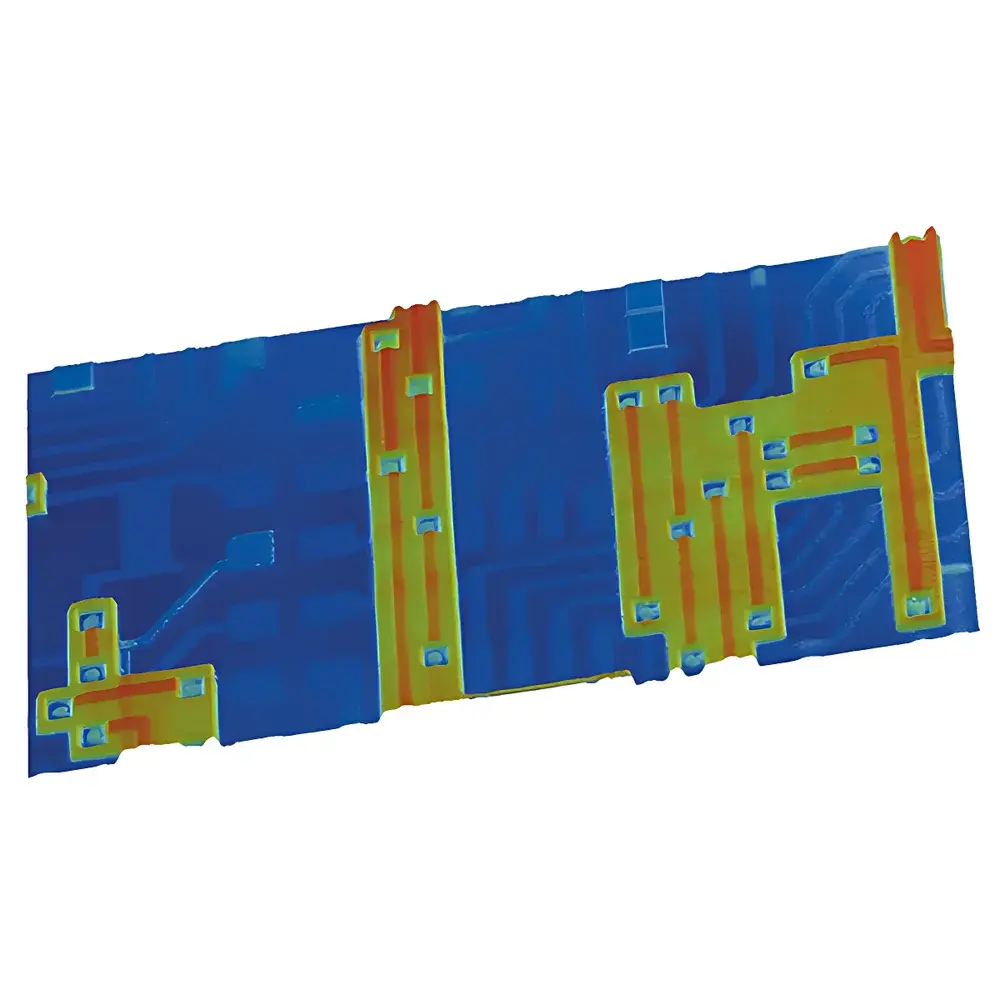
- Semiconductor packaging: Verification of die attach layer uniformity, underfill fillet geometry, and redistribution layer (RDL) step coverage
- MEMS fabrication: Critical dimension (CD) metrology of etched cavities, comb-drive gaps, and release-hole depths with <5 Å repeatability
- Microfluidics: Depth profiling of PDMS or PMMA channels (10–500 µm wide, 1–100 µm deep) and surface roughness assessment of bonding interfaces
- Optical coatings: Thickness mapping of anti-reflective or high-reflection stacks on plano-convex lenses and laser optics substrates
FAQ
What is the minimum resolvable step height on the Dektak XT?
The system achieves vertical resolution of 1 Å (0.1 nm) under optimal conditions; practical step height detection limit is typically ~5 Å for single-scan measurements on clean, stable surfaces.
Can the Dektak XT measure transparent or multilayer films?
Yes—when combined with optical reflectance calibration or reference standards, it quantifies physical step height at film interfaces, independent of optical properties.
Is tip wear monitored automatically during operation?
Vision64 includes tip life tracking based on cumulative scan distance and force history; users receive alerts when tip replacement is recommended per Bruker’s maintenance schedule.
Does the system support automated wafer mapping?
With optional motorized XY stage and Vision64 AutoMap module, up to 25 locations per 50 mm wafer can be programmed for unattended multi-site profiling.
How is calibration verified between scheduled service intervals?
Built-in self-test routines validate Z-axis linearity and noise floor daily; certified reference standards are used for periodic performance qualification per ISO/IEC 17025 internal audit requirements.