ZEISS Primotech Multimedia Interactive Teaching Microscopy System
| Brand | ZEISS |
|---|---|
| Origin | Germany |
| Manufacturer Status | Authorized Distributor |
| Product Origin | Imported |
| Model | Primotech |
| Mounting Type | Upright |
| Image Analysis System | Integrated |
| Total Magnification Range | 50×–1000× |
| Eyepiece | 10× |
| Objective Lenses | 5×, 10×, 20×, 40×, 50×, 63×, 100× (user-selectable combination) |
Overview
The ZEISS Primotech Multimedia Interactive Teaching Microscopy System is an upright metallurgical and materials microscopy platform engineered for precision imaging, quantitative analysis, and collaborative education in academic laboratories and industrial quality control environments. Built on ZEISS’s legacy of optical excellence, the system employs high-NA achromatic and apochromatic objective optics with parfocal and parcentric alignment to ensure consistent focus and field centering across magnifications. Its modular architecture supports simultaneous transmitted and reflected light illumination paths—enabling seamless characterization of both opaque metallic specimens (e.g., polished metallographic sections) and semi-transparent or transparent samples (e.g., PCBs, thin films, polymer foils). The system operates on a robust mechanical stage with motorized or manual ESD-safe options, integrated 3 MP sensor housed within the observation tube to eliminate external cabling and maintain optical path integrity, and thermally stable LED illumination delivering constant color temperature (5700 K ± 150 K) across intensity adjustments—critical for reproducible photometric measurements and long-duration classroom demonstrations.
Key Features
- Encoded 5-position objective turret with automatic magnification recognition—eliminates manual input errors and synchronizes calibration metadata with each image acquisition.
- Dual-path illumination system: configurable Koehler-based reflected-light path for metallurgical inspection and adjustable transmitted-light path with condenser (optional) for thin-section or semiconductor wafer analysis.
- ESD-compliant stage variants available—certified to IEC 61340-5-1 for safe handling of electrostatic-sensitive devices (ESDs), including bare PCBAs and microelectronic components.
- Integrated 3-megapixel CMOS camera sealed within the microscope body—ensures dust resistance, thermal stability, and alignment persistence under continuous lab use.
- Modular optical configurations: Primotech D/A (dual-illumination), Primotech D/POL (polarized & conoscopy-ready), and base Primotech models support application-specific deployment without hardware redundancy.
- LED illumination with intelligent thermal management—maintains <±0.5% intensity drift over 8-hour operation and delivers uniform illumination across full field of view (FOV ≥ 22 mm).
Sample Compatibility & Compliance
The Primotech system accommodates specimens up to 34 mm in height when configured without condenser, making it suitable for thick-section metallurgical mounts, castings, and additive-manufactured parts. Its dual-illumination capability allows direct comparison of phase contrast, brightfield, darkfield, and polarized modalities on identical regions of interest—essential for ASTM E112 grain size evaluation, ISO 643 ferrite/pearlite quantification, and USP particulate analysis in pharmaceutical excipients. All optical components comply with DIN ISO 10110 surface quality standards; LED light sources meet IEC 62471 photobiological safety Class 1 requirements. The system architecture supports GLP/GMP-aligned workflows through audit-trail-enabled software logging and user-access controls compatible with FDA 21 CFR Part 11 compliance frameworks when deployed with validated Matscope configuration.
Software & Data Management
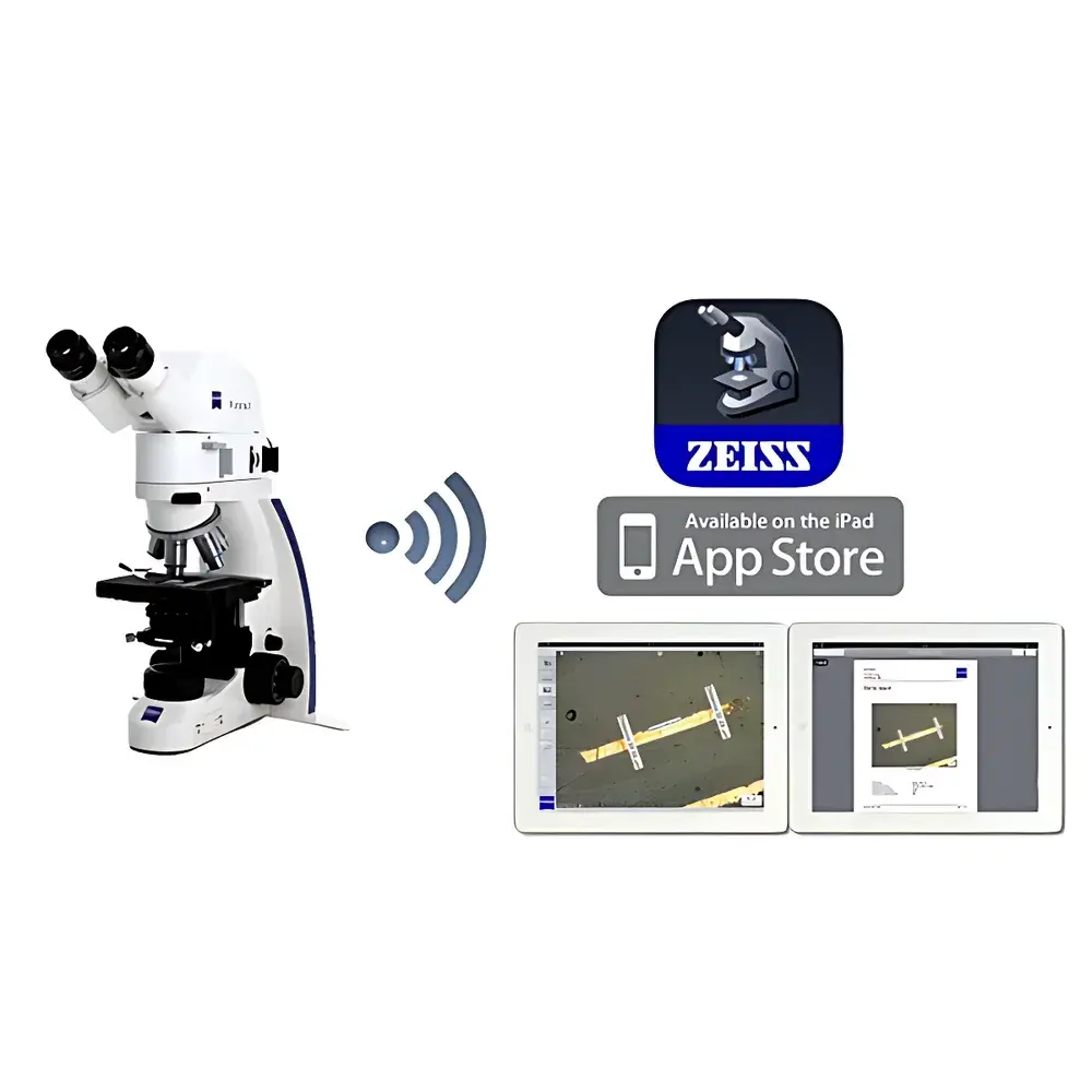
ZEISS Matscope—a free, cross-platform imaging application—enables wireless connection to multiple Primotech units via IEEE 802.11ac Wi-Fi. It provides real-time image/video streaming to tablets or laptops, synchronized multi-user annotation, and automated metadata embedding (magnification, objective ID, illumination mode, timestamp). Core analytical functions include calibrated 2D length/area measurement, multi-phase segmentation with threshold-based classification, extended depth-of-field (EDF) stacking, semi-automated coating thickness calculation per ISO 20631, and customizable report generation with embedded scale bars and NIST-traceable calibration references. All measurement data exports to CSV, TIFF, or PDF formats with embedded EXIF tags—including objective NA, pixel size, and exposure parameters—for traceability in ISO/IEC 17025-accredited labs.
Applications
- University-level materials science instruction: real-time student sharing of live microstructures during lectures on phase transformations, corrosion mechanisms, or composite fiber orientation.
- Industrial QC labs: rapid verification of solder joint integrity, void fraction in thermal interface materials, and inclusion counting in aluminum alloys per ASTM E45.
- Geoscience education: petrographic analysis of thin sections using conoscopy mode (with D/POL variant) and birefringence quantification via standardized DIN compensator slots.
- Electronics manufacturing: simultaneous top-side (reflected) and substrate-side (transmitted) inspection of vias, traces, and delamination in multilayer PCBs.
- Research labs: time-lapse monitoring of recrystallization kinetics or grain boundary migration under controlled thermal stages (compatible with third-party heating platforms).
FAQ
Is the Primotech system compliant with ISO/IEC 17025 documentation requirements?
Yes—when deployed with Matscope’s audit trail module enabled and user roles assigned, all image acquisitions, measurements, and report generations are timestamped, user-attributed, and immutable, satisfying clause 7.5.2 of ISO/IEC 17025:2017.
Can the system perform quantitative grain size analysis per ASTM E112?
Yes—the integrated Matscope software includes automated linear intercept and planimetric methods with selectable test line lengths and grid densities, fully aligned with ASTM E112 Annex A1 guidelines.
What is the maximum working distance supported for thick specimens?
Up to 34 mm when configured without condenser; optional long-working-distance objectives (e.g., 5×/WD 25.5 mm) extend usable clearance while preserving resolution.
Does Matscope support remote calibration verification?
Yes—users can load NIST-traceable stage micrometer images to auto-validate pixel-to-micron scaling at any magnification, with results logged in the audit trail.
Are ESD-safe components certified to industry standards?
The ESD stage option complies with IEC 61340-5-1 and includes resistivity testing documentation per ANSI/ESD S20.20, ensuring discharge rates <100 ns for sensitive semiconductor handling.


