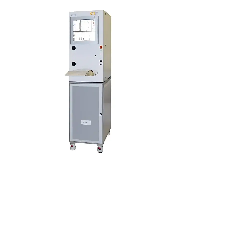
KLA-Tencor Candela CS1 Optical Surface Analyzer
| Origin | USA |
|---|---|
| Manufacturer Type | Authorized Distributor |
| Origin Category | Imported |
| Model | CS1 |
| Pricing | Available Upon Request |
| Substrate Diameter Range | 2 in. – 200 mm |
| Substrate Thickness Range | 350 μm – 1,100 μm |
| Material Compatibility | Opaque or transparent polished surfaces with ≥10% light scattering efficiency |
| Defect Detection Sensitivity | 0.3 μm PSL sphere equivalent (≥95% capture rate on bare Si) |
| Minimum Detectable Features | Scratches (100 μm × 0.1 μm × 50 Å), Pits (20 μm Ø × 50 Å depth), Stains (20 μm Ø × 10 Å thickness) |
| Signal Threshold | Defect signal amplitude >3× peak-to-valley background noise |
Overview
The KLA-Tencor Candela CS1 Optical Surface Analyzer is a high-sensitivity, non-contact inspection system engineered for rapid, quantitative detection and classification of surface defects on polished semiconductor wafers, optical substrates, and precision-engineered components. Leveraging dark-field laser scattering (DFLS) technology, the CS1 illuminates the sample surface at oblique angles using collimated monochromatic light and captures scattered photons with a high-numerical-aperture imaging lens and low-noise CCD detector. This architecture enables sub-micron particle detection without physical contact or surface preparation—critical for maintaining wafer integrity in front-end-of-line (FEOL) process control. Unlike interferometric profilometers or stylus-based systems, the CS1 operates exclusively in scatter-mode, making it purpose-built for defect-centric metrology rather than topographic reconstruction. Its design complies with industry-standard requirements for inline and offline wafer qualification in cleanroom environments (Class 100 or better), supporting both R&D validation and high-volume manufacturing (HVM) monitoring.
Key Features
- Dark-field laser scattering optics optimized for high signal-to-noise ratio (SNR) detection across broad substrate sizes—from 2-inch wafers to full 200 mm (8-inch) diameter discs.
- Automated defect classification engine trained on statistically representative libraries of particles, scratches, pits, stains, and bumps—enabling traceable categorization per SEMI D39 and SEMI E142 guidelines.
- Real-time acquisition with configurable scan resolution (down to 1 µm/pixel) and adjustable illumination intensity to accommodate varying surface reflectivity and scattering cross-sections.
- Integrated motion control with high-precision air-bearing XY stage and Z-axis focus servo, ensuring repeatable positioning accuracy ≤ ±0.5 µm over full travel range.
- Robust mechanical architecture with thermal mass stabilization and vibration isolation, enabling stable operation in standard fab environments without active damping systems.
- Modular software interface supporting recipe-driven inspection, multi-site mapping, and pass/fail binning based on user-defined defect density thresholds (e.g., particles/cm²).
Sample Compatibility & Compliance
The CS1 accommodates rigid, flat, polished substrates within defined dimensional and optical constraints: diameters from 50.8 mm (2 in.) to 200 mm; thicknesses between 350 µm and 1,100 µm; and surface materials exhibiting ≥10% diffuse scattering of incident 633 nm laser light. Compatible substrates include silicon, sapphire, fused silica, quartz, and polished metals such as stainless steel or aluminum—provided surface roughness (Ra) remains below 0.5 nm and no residual organic films interfere with scattering signatures. The system meets electromagnetic compatibility (EMC) requirements per FCC Part 15 Class A and CE Directive 2014/30/EU. All measurement data logs are timestamped and stored with audit-trail metadata compliant with ISO/IEC 17025:2017 and FDA 21 CFR Part 11 when operated under validated software configuration.
Software & Data Management
The CS1 runs on KLA-Tencor’s proprietary CandelaVision™ software suite, which provides full control over acquisition parameters, defect review workflows, and statistical process control (SPC) charting. Raw scatter images and classified defect lists are saved in HDF5 format with embedded calibration metadata—including lens distortion coefficients, stage encoder offsets, and laser power history. Export options include CSV (for SPC integration), XML (for MES/ERP ingestion), and SEMI E142-compliant GDSII-compatible defect maps. Audit trails record all operator actions, parameter changes, and software updates with digital signature verification. Optional modules support automated reinspection of flagged sites via coordinate-based navigation and integration with KLA’s Panorama™ analytics platform for cross-tool correlation.
Applications
- Semiconductor wafer incoming inspection and post-CMP/post-etch defect screening.
- Optical component qualification for laser optics, EUV mask blanks, and lithography lenses.
- Quality assurance of MEMS substrates, compound semiconductor wafers (GaN, SiC), and advanced packaging interposers.
- Process development support for cleaning, polishing, and thin-film deposition steps where surface contamination or micro-scratching impacts yield.
- Failure analysis root-cause tracing through comparative defect morphology analysis across process lots.
FAQ
What substrate materials are supported by the CS1?
Silicon, sapphire, fused silica, quartz, and polished metallic substrates—provided they exhibit ≥10% diffuse scattering at 633 nm and maintain surface roughness (Ra) < 0.5 nm.
Can the CS1 detect subsurface defects?
No. The CS1 detects only surface-scattered light; it is not designed for subsurface or bulk defect characterization.
Is the system compatible with cleanroom Class 10 environments?
Yes—when equipped with optional HEPA-filtered purge and static-dissipative enclosure upgrades, the CS1 meets ISO Class 4 (Class 10) cleanroom operational standards.
Does the software support automated reporting per ISO 9001 requirements?
Yes. Report templates can be customized to include calibration status, operator ID, environmental conditions, and measurement uncertainty budgets aligned with ISO/IEC 17025 Annex A.3.
How frequently does the system require recalibration?
Annual traceable calibration is recommended; however, daily performance verification using NIST-traceable PSL reference standards is required per internal quality protocols.


