Scientech 12-inch Silicon Wafer Reclaim System
| Brand | Scientech |
|---|---|
| Origin | Taiwan |
| Manufacturer Type | Authorized Distributor |
| Domestic Product Classification | Yes |
| Model | 12-inch |
| Pricing | Available Upon Request |
Overview
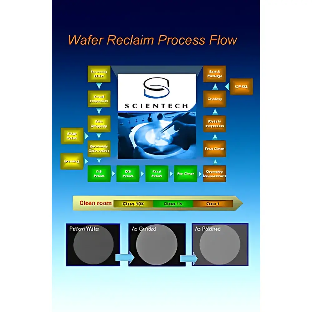
The Scientech 12-inch Silicon Wafer Reclaim System is a dedicated semiconductor process tool engineered for the high-precision regeneration of used 300 mm (12-inch) silicon wafers. Unlike inspection or metrology instruments, this system performs full-cycle wafer reclamation—comprising sequential cleaning, surface defect removal, oxide stripping, polishing, and final particle-free rinsing—to restore wafers to specifications suitable for reuse in non-critical front-end or back-end fabrication steps. The system operates on a dual-line architecture: one optimized for copper-containing device wafers (e.g., post-CMP or post-etch residues), and the other configured for non-copper substrates (e.g., bare Si, SiO₂, or nitride-based wafers). This segregation ensures cross-contamination control, chemical compatibility, and process stability—critical requirements under ISO 14644-1 Class 5 cleanroom environments and aligned with SEMI S2/S8 safety and environmental guidelines.
Key Features
- Dual independent processing lines: Separated copper and non-copper reclaim pathways to prevent metal contamination and ensure material-specific chemistry optimization.
- Sub-micron thickness control: Capable of controlled material removal ≤ 0.5 µm per cycle, preserving wafer flatness (TTV < 0.3 µm) and global planarity (Warp < 1 µm) as verified by optical interferometry.
- High reclaim yield: Achieves >92% successful regeneration rate for standard 12-inch prime-grade wafers with ≤ 100 nm particle counts < 50/cm² post-reclaim (per SEMI F57).
- Short turnaround time: Standard cycle time from intake to certified output is ≤ 72 hours, including QA release documentation and traceability logs.
- Integrated process monitoring: Real-time logging of critical parameters—including bath temperature (±0.1 °C), pH (±0.02), conductivity (±0.5 µS/cm), and rinse resistivity (>18.2 MΩ·cm)—with automated alerts for deviation thresholds.
- Modular design compliant with fab facility integration standards: Supports SECS/GEM communication protocols and interfaces with MES via Ethernet/IP for lot-level data exchange.
Sample Compatibility & Compliance
The system accepts standard 300 mm silicon wafers with nominal thickness of 775 ± 25 µm, including those with patterned or unpatterned surfaces, thermal oxide layers (up to 2 µm), and low-k dielectrics. It is compatible with wafers bearing residual photoresist, metal films (Cu, Al, W, TiN), and etch residues typical of logic, memory, and power device manufacturing. All wet processes comply with SEMI C1–C36 chemical handling standards and are validated for residue limits per SEMI F38 (metallic contamination) and SEMI F57 (particle count). Full traceability records—including wafer ID, process step timestamps, chemical lot numbers, and operator verification—are retained for ≥24 months to support internal quality audits and GLP/GMP-aligned documentation practices.
Software & Data Management
The embedded control software provides recipe-driven operation with version-controlled process sequences, user-access levels (admin/operator/technician), and electronic signature capability meeting FDA 21 CFR Part 11 requirements. Audit trails record all parameter changes, manual overrides, and QA approvals with immutable timestamps. Export formats include CSV and XML for integration into enterprise LIMS or QMS platforms. All system logs are encrypted at rest and support TLS 1.2+ secure transmission—ensuring compliance with ISO/IEC 27001 information security frameworks applicable to semiconductor supply chain data handling.
Applications
- Cost-effective reuse of monitor wafers in lithography, etch, and deposition tool qualification.
- Pre-production substrate preparation for pilot line development and process window characterization.
- Recycling of test wafers from reliability stress testing (HTOL, ESD, TDDB) where electrical performance is not required.
- Supporting sustainability initiatives by reducing virgin wafer consumption and lowering CO₂ footprint per wafer processed (verified via LCA per ISO 14040).
- Enabling rapid ramp-up for new technology nodes by bridging wafer supply gaps during initial material qualification phases.
FAQ
Is the reclaimed wafer suitable for front-end-of-line (FEOL) processing?
Reclaimed wafers meet specifications for non-critical FEOL applications such as dummy runs, chamber conditioning, and tool matching—but are not certified for gate oxide or epitaxial layer growth without additional customer-specific qualification.
What documentation accompanies each reclaimed wafer lot?
Each shipment includes a Certificate of Conformance (CoC) listing wafer IDs, reclaim date, process sequence ID, final particle count (per SEMI F57), surface roughness (Ra < 0.2 nm), and trace metal analysis (ICP-MS data per SEMI F38).
Can the system be integrated into an existing fab’s automation infrastructure?
Yes—the system supports SECS/GEM v5.0 and provides OPC UA server functionality for seamless connectivity with host MES, AMHS, and equipment monitoring systems.
Does Scientech provide on-site validation support?
Scientech partners with qualified third-party labs accredited to ISO/IEC 17025 for IQ/OQ/PQ execution and offers remote technical assistance for protocol development and report review.
Related Products


