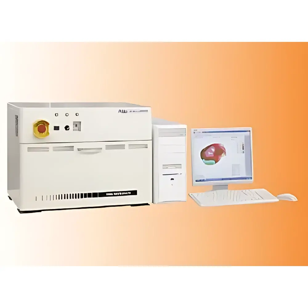
Toho FLX-2320-S Thin-Film Stress Analyzer
| Brand | Toho |
|---|---|
| Origin | Japan |
| Model | FLX-2320-S |
| Application | In-situ and ex-situ thin-film stress measurement on semiconductor wafers up to 8 inches (200 mm) |
| Temperature Control Range | −65 °C to +500 °C |
| Dual-Laser Source | Visible (e.g., 635 nm) and Near-Infrared (e.g., 785 nm) |
| Data Export | CSV, Excel (.xlsx), XML |
| Software Compliance | Audit trail-ready configuration supporting GLP/GMP-aligned documentation workflows |
Overview
The Toho FLX-2320-S Thin-Film Stress Analyzer is an engineered metrology platform designed for quantitative, non-contact curvature-based stress evaluation of thin films deposited on planar substrates—primarily silicon, sapphire, SiC, and glass wafers up to 200 mm (8-inch) diameter. It operates on the Stoney equation principle, where localized film-induced substrate curvature is measured via high-resolution laser deflection scanning, enabling calculation of biaxial stress with sub-mPa resolution. The system supports both as-deposited and thermally cycled stress characterization, making it essential for process development, reliability qualification, and failure analysis in front-end-of-line (FEOL) and back-end-of-line (BEOL) semiconductor manufacturing. Its dual-wavelength laser architecture ensures optimal signal-to-noise ratio across diverse film–substrate combinations—including low-reflectivity metals (e.g., TiN, TaN), high-index dielectrics (e.g., SiNx, SiO2), and transparent conductive oxides—without requiring manual optical alignment or coating.
Key Features
- Dual-laser scanning system: Automatically selects between visible (635 nm) and near-infrared (785 nm) sources based on real-time reflectivity and surface absorption characteristics—minimizing measurement artifacts from interference, scattering, or thermal lensing.
- Integrated thermal chamber: Precisely controlled temperature ramping from −65 °C to +500 °C enables dynamic stress profiling during thermal cycling, supporting studies of coefficient of thermal expansion (CTE) mismatch, stress relaxation kinetics, and phase-transition–induced stress evolution.
- Material property database: Pre-loaded elastic modulus (E), Poisson’s ratio (ν), and CTE values for >120 standard semiconductor and MEMS-relevant materials—including crystalline Si, fused quartz, Al2O3, SiC, and common PVD/CVD stack components—with user-defined entry fields for proprietary alloys or novel low-k dielectrics.
- High-fidelity 3D stress mapping: Generates spatially resolved stress topography with ≤50 µm lateral resolution over full wafer area; outputs iso-stress contours, gradient vectors, and radial/tangential stress components for mechanical modeling input.
- Calibration traceability: Factory-certified curvature sensitivity ≤0.02 m−1; optional NIST-traceable calibration kit available for ISO/IEC 17025-compliant lab accreditation.
Sample Compatibility & Compliance
The FLX-2320-S accommodates flat, rigid substrates with diameters from 50 mm to 200 mm and thicknesses ranging from 200 µm to 2 mm. It supports bare wafers, patterned devices (with feature sizes ≥5 µm), and multi-layer stacks—including ALD-grown HfO2, PECVD SiNx, electroplated Cu interconnects, and spin-on carbon hard masks. All hardware and software modules comply with SEMI S2/S8 safety standards and are compatible with cleanroom Class 100 (ISO 5) environments. Data acquisition and storage meet FDA 21 CFR Part 11 requirements when configured with electronic signature-enabled software licensing and encrypted audit logs.
Software & Data Management
The proprietary FLX-Studio software provides a deterministic, scriptable interface for measurement protocol definition, real-time curvature visualization, and comparative stress analytics. Each session records full metadata—including ambient pressure, chamber purge gas composition (N2/Ar), temperature ramp rate, laser power history, and stage position calibration status. Export formats include IEEE-compliant CSV, Microsoft Excel (.xlsx), and XML schemas compatible with MATLAB, Python (pandas), and JMP for statistical process control (SPC) integration. Version-controlled software updates are delivered via secure HTTPS with SHA-256 integrity verification; release notes document all changes per ISO 9001 design change control procedures.
Applications
- Process optimization of PVD sputtering, CVD, and ALD deposition tools—correlating chamber pressure, RF power, and precursor flow with residual compressive/tensile stress.
- Evaluation of post-deposition anneal effects on stress redistribution in BEOL metal/dielectric stacks.
- Qualification of low-thermal-budget encapsulation layers for advanced packaging (e.g., Fan-Out Wafer-Level Packaging).
- Fundamental research on stress–strain coupling in 2D material heterostructures (e.g., MoS2/h-BN) and ferroelectric oxide thin films.
- Root-cause analysis of wafer bow, crack propagation, and delamination in high-aspect-ratio TSV structures.
FAQ
What wafer sizes does the FLX-2320-S support?
The system is optimized for 50 mm to 200 mm (8-inch) wafers. For 300 mm (12-inch) substrates, Toho recommends the FLX-3300 model.
Can the system measure stress on patterned wafers?
Yes—provided minimum feature pitch exceeds 5 µm and surface topography variation remains below ±1 µm peak-to-valley; automated focus tracking compensates for local height variations.
Is the elastic modulus database modifiable by the user?
Yes. Users may import custom material properties via CSV templates, including temperature-dependent E(T) and ν(T) functions for transient thermal stress modeling.
Does the software support automated pass/fail criteria for production lots?
Yes. Threshold-based flagging, histogram generation, and Cp/Cpk reporting are configurable within the measurement sequence editor.
How is system calibration maintained over time?
A quarterly self-diagnostic routine verifies laser alignment, stage repeatability, and thermal sensor drift; full recalibration is recommended every 12 months or after major maintenance events.


