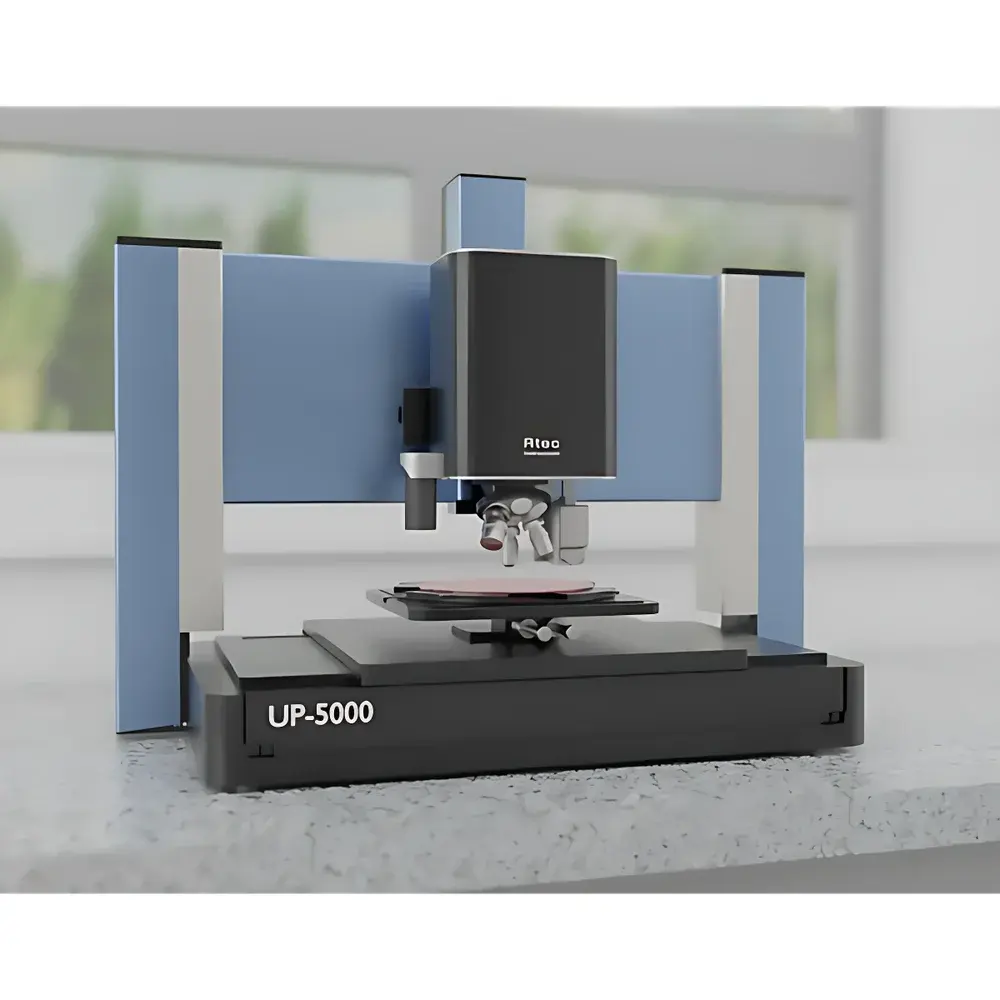
Rtec UP-WLI White Light Interferometric 3D Surface Profilometer
| Brand | Rtec |
|---|---|
| Origin | Switzerland |
| Model | UP-WLI |
| Imaging Modes | White Light Interferometry (WLI), Confocal Microscopy, Dark-Field Microscopy, Bright-Field Microscopy |
| Vertical Measurement Range | up to 100 mm |
| XY Stage Resolution | 0.1 µm |
| Standard Motorized Stage | 150 × 150 mm (optional 210 × 310 mm) |
| Tilt Stage | ±6° |
| Automated Stitching Capability | Yes |
| Head Options | Sigma Head (WLI-only) / Lambda Head (WLI + Confocal + Dark-Field + Bright-Field) |
| Compliance | ASTM E2923, ISO 25178-2, ISO 4287, USP <1059>, FDA 21 CFR Part 11 (software audit trail enabled) |
Overview
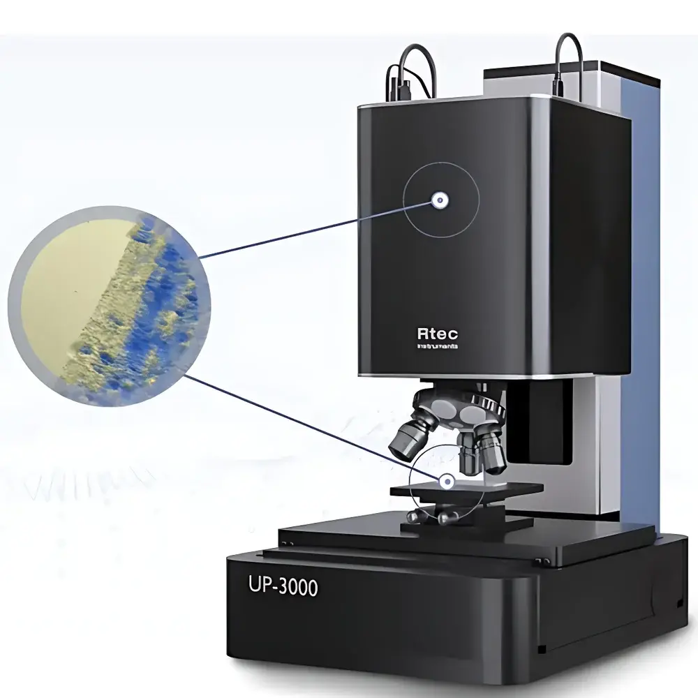
The Rtec UP-WLI White Light Interferometric 3D Surface Profilometer is an engineered metrology platform designed for nanoscale topographic characterization of diverse surfaces under a single optical head architecture. It operates on the principle of low-coherence interferometry—where broadband white light generates localized interference fringes only at the focal plane—enabling sub-nanometer vertical resolution and exceptional lateral repeatability. Unlike conventional profilometers limited to reflective or planar samples, the UP-WLI integrates four complementary optical imaging modalities—white light interferometry (WLI), rotating-disk confocal microscopy, dark-field, and bright-field microscopy—within one mechanically stable, motorized optical head (Lambda configuration). This multi-modal convergence allows quantitative surface analysis across materials with varying optical properties: transparent thin films, highly absorbing substrates (e.g., carbon-based coatings), curved geometries (e.g., lenses, bearings), and microstructured features (e.g., MEMS channels, biochip surfaces). The system’s core architecture eliminates mechanical reconfiguration between techniques, ensuring spatial registration accuracy better than 0.3 µm between modes—critical for correlative metrology workflows in R&D and quality control environments.
Key Features
- Multi-modal optical head (Lambda): seamless switching among WLI, confocal, dark-field, and bright-field imaging via software command—no manual lens or filter changes required.
- Vertical measurement range up to 100 mm with calibrated Z-axis linearity < ±0.1% over full range; vertical resolution < 0.1 nm (RMS noise, typical).
- Motorized XYZ stage with 0.1 µm encoder resolution and programmable tilt (±6°) for oblique-angle measurements and wafer-level metrology.
- Automated large-area stitching: supports mosaic acquisition across >100 mm² with sub-pixel registration and intensity normalization.
- Dual-head option: Sigma head dedicated to ultra-high-speed WLI (up to 100 fps frame rate for dynamic surface monitoring); Lambda head optimized for multi-contrast correlative analysis.
- Thermally stabilized optical path and active vibration isolation compatibility ensure measurement stability in non-dedicated lab environments.
Sample Compatibility & Compliance
The UP-WLI accommodates samples ranging from silicon wafers and optical lenses to biological membranes, polymer coatings, and textured metal substrates—regardless of reflectivity, transparency, or curvature. Its adaptive illumination and dynamic range optimization algorithms suppress saturation on specular surfaces while recovering signal from low-reflectance regions (e.g., DLC, graphene, hydrogels). All hardware and firmware comply with CE marking requirements. Software validation packages support GLP/GMP environments: full 21 CFR Part 11 compliance includes electronic signatures, role-based access control, immutable audit trails, and data integrity logging. Surface parameter calculations adhere to ISO 25178-2 (areal surface texture), ISO 4287 (profile roughness), ASTM E2923 (thin-film thickness by interferometry), and USP (surface characterization of pharmaceutical delivery devices).
Software & Data Management
The proprietary Rtec Surface Analysis Suite (v6.2+) provides unified control, real-time visualization, and standards-compliant reporting. It includes automated feature detection (e.g., step height, pit volume, grain boundary delineation), batch processing for production lot analysis, and customizable report templates exportable to PDF, CSV, and STEP AP210 formats. Raw interferograms and confocal z-stacks are stored in vendor-neutral HDF5 containers with embedded metadata (acquisition parameters, calibration certificates, user annotations). Data provenance is preserved through hierarchical versioning—each exported parameter traceably links back to raw frames, instrument configuration, and environmental logs (temperature, humidity timestamps). Integration with LIMS and MES systems is supported via RESTful API and OPC UA interfaces.
Applications
- Thin-film metrology: non-contact thickness and uniformity mapping of dielectric stacks, anti-reflective coatings, and semiconductor passivation layers (0.5 nm–50 µm range).
- Wear & tribology: 3D volumetric wear loss quantification on bearing races, piston rings, and orthopedic implants using pre/post-test surface registration.
- Microfabrication QA: sidewall angle, trench depth, and mask alignment verification on MEMS, photonic crystals, and microfluidic chips.
- Biomedical surfaces: roughness evolution of dental implants, endothelial cell adhesion substrates, and drug-eluting stent coatings.
- Failure analysis: identification and quantification of coating delamination, fatigue cracks, and abrasive scratches on aerospace alloys and turbine blades.
- Optics manufacturing: form error assessment of aspheric lenses, diffractive optical elements, and laser mirror substrates.
FAQ
What surface types can be measured without sample preparation?
Transparent substrates (glass, sapphire), metals, ceramics, polymers, and biological films—provided they exhibit sufficient optical contrast. No conductive coating or vacuum is required.
Is the system compatible with cleanroom Class 100 environments?
Yes. Optional HEPA-filtered air purge and static-dissipative stage components meet ISO 14644-1 Class 5 specifications.
Can the UP-WLI measure step heights below 1 nm?
Yes. With phase-shifting WLI and thermal drift compensation, sub-0.2 nm step height repeatability is achievable on calibrated reference artifacts.
How is traceability maintained for ISO/IEC 17025 accreditation?
NIST-traceable step height and roughness standards are included; full calibration documentation, uncertainty budgets, and inter-laboratory comparison reports are provided per IEC 17025 Annex A.3.
Does the software support custom algorithm development?
Yes. Python SDK and C++ API enable integration of proprietary analysis routines—including machine learning-based defect classification—into the native workflow engine.


