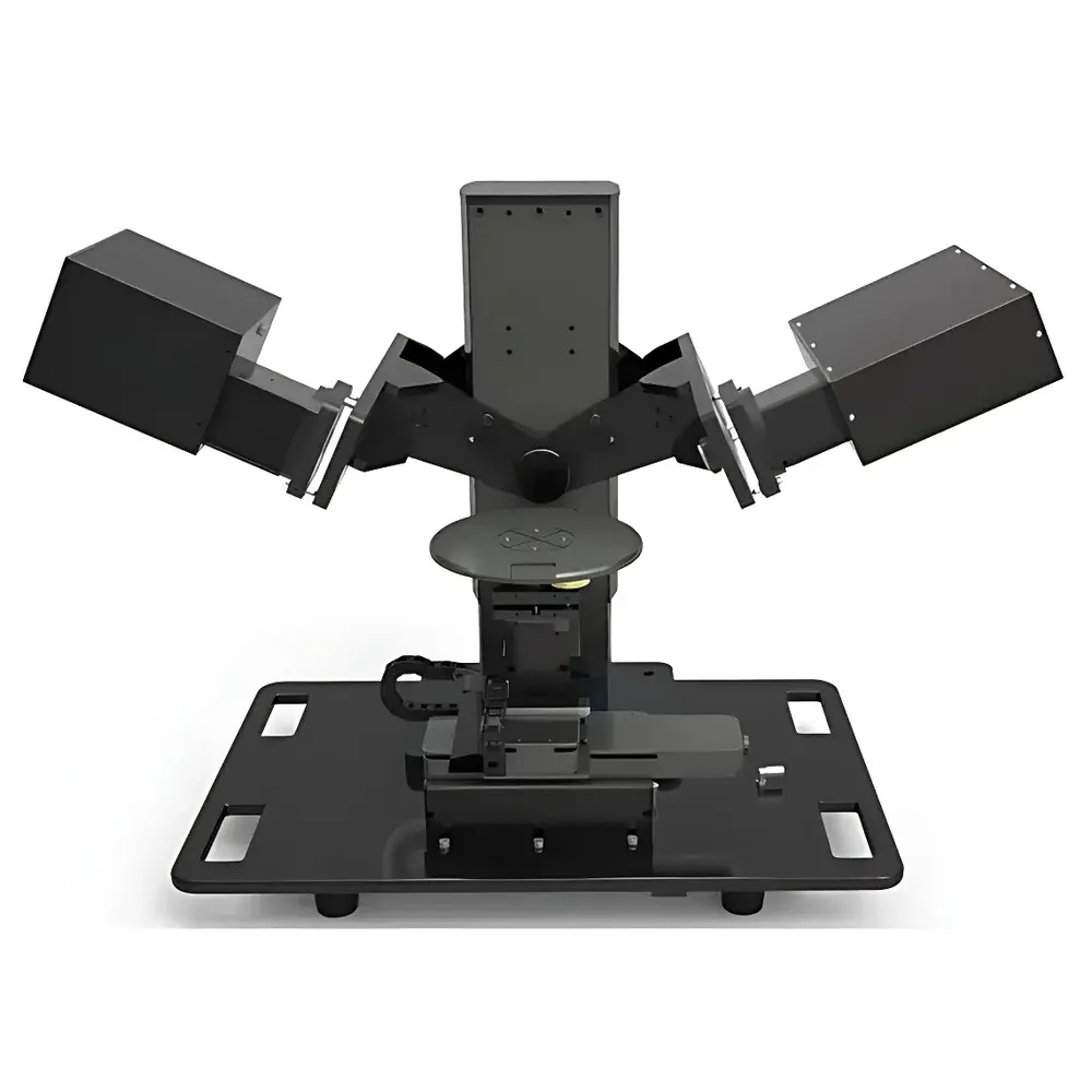
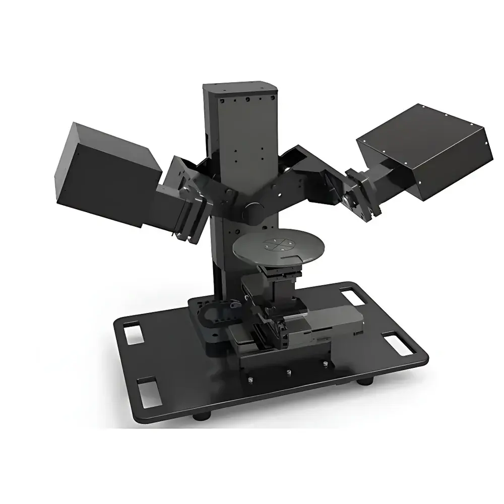
KJ GROUP SE-L Spectroscopic Ellipsometer
| Brand | KJ GROUP |
|---|---|
| Origin | Liaoning, China |
| Manufacturer Type | Authorized Distributor |
| Origin Category | Domestic (China) |
| Model | SE-L |
| Pricing | Available Upon Request |
| Light Source | Deuterium + Tungsten-Halogen Composite Lamp |
| Spectral Range | 193–2500 nm (configurable sub-bands: V: 380–1000 nm |
| UV | 245–1000 nm |
| XN | 210–1650 nm |
| DN+ | 193–2500 nm) |
| Incidence Angle Range | 45°–90° (motorized auto-adjustment) |
| Spot Size | 2–3 mm (macro), 200 µm (micro) |
| Measurement Time per Point | 0.5–5 s |
| Repeatability | ±0.01 nm (film thickness) |
| Auto-Focusing | Integrated motorized Z-stage with real-time feedback |
| Sample Stage | Motorized XY mapping up to 100 × 100 mm (optional) |
| Max sample diameter | 200 mm |
| Optical Configuration | Phase-Compensated Rotating Compensator (PCRSA) |
| Output Parameters | Ψ(λ), Δ(λ), R(λ), T(λ), n(λ), k(λ), C(λ), S(λ) |
| Software | EllipsoVision™ v5.x with GLP-compliant audit trail, ISO/IEC 17025-aligned data handling, and FDA 21 CFR Part 11-ready optional modules |
Overview
The KJ GROUP SE-L Spectroscopic Ellipsometer is a fully automated, high-precision optical metrology platform engineered for non-destructive, model-based characterization of thin films and nanostructured surfaces. It operates on the fundamental principle of spectroscopic ellipsometry—measuring the change in polarization state (amplitude ratio Ψ and phase difference Δ) of light reflected from a sample across a broad spectral range. Unlike intensity-based reflectometry, ellipsometry delivers intrinsic sensitivity to sub-nanometer film thickness, complex refractive index (n + ik), and interfacial roughness—even for transparent, absorbing, or multilayered systems. The SE-L implements a phase-compensated rotating compensator (PCRSA) architecture, eliminating moving polarizer/analyzer components and enabling high-speed, high-stability acquisition of full Ψ(λ)/Δ(λ) spectra with minimal instrumental artifacts. Its dual-lamp illumination system (deuterium for deep-UV stability and tungsten-halogen for NIR continuity) ensures spectrally uniform signal-to-noise performance from 193 nm to 2500 nm—covering critical bands for SiO₂ gate dielectrics, III–V epitaxial layers (e.g., GaN, AlGaN), transparent conductive oxides (ITO, AZO), organic photovoltaics, and biofunctional coatings.
Key Features
- Fully motorized optical platform: automated incidence angle adjustment (45°–90°), precision Z-axis autofocus with closed-loop feedback, and programmable XY mapping stage (standard 100 × 100 mm travel, scalable to 200 mm wafers)
- High-fidelity spectral acquisition: PCRSA modulation enables <10 ms spectral point dwell time, supporting rapid single-point measurements (0.5–5 s) and high-resolution spatial mapping without compromise in data fidelity
- Modular spectral configuration: Interchangeable optical paths support user-selectable ranges—V-band (380–1000 nm), UV-band (245–1000 nm), extended NIR XN-band (210–1650 nm), or full deep-UV to NIR DN+-band (193–2500 nm)
- Dual-spot optics: Macro-mode (2–3 mm spot) for rapid uniformity screening; micro-mode (200 µm spot) for localized analysis of patterned devices, trenches, or heterogeneous surfaces
- EllipsoVision™ software suite: Intuitive wizard-driven workflow for optical modeling, multi-layer stack fitting, and dispersion analysis—with built-in validation tools for parameter identifiability and covariance assessment
- Hardware-expandable architecture: Optional integration of environmental modules—including vacuum chamber (10⁻⁵ mbar), temperature-controlled stage (RT to 600 °C), transmission adsorption cell, and motorized mapping extension kits
Sample Compatibility & Compliance
The SE-L accommodates rigid and flexible substrates up to 200 mm in diameter—including silicon wafers, glass slides, quartz crystals, polymer foils, and metallic coupons. Its non-contact, non-destructive methodology complies with ASTM E1939 (Standard Guide for Spectroscopic Ellipsometry), ISO 15382 (Optical methods for thin film thickness measurement), and SEMI MF2038 (Ellipsometric measurement of thin film properties). When configured with audit-trail-enabled software and electronic signature modules, the system supports GLP and GMP environments per FDA 21 CFR Part 11 requirements. All calibration protocols are traceable to NIST-certified reference standards (e.g., Si/SiO₂ witness wafers, certified optical density filters), and uncertainty budgets are documented per ISO/IEC 17025 Annex A.5 guidelines.
Software & Data Management
EllipsoVision™ v5.x provides a unified interface for instrument control, real-time data visualization, optical modeling, and report generation. The software includes over 300 pre-characterized material dispersion models (Cauchy, Sellmeier, Tauc-Lorentz, Cody-Lorentz, B-spline), layered geometry templates (graded interfaces, roughness zones, anisotropic slabs), and iterative regression engines (Levenberg-Marquardt, Nelder-Mead). Raw Ψ/Δ spectra are stored in HDF5 format with embedded metadata (timestamp, stage position, lamp status, ambient conditions). Export options include CSV, XML, and PDF reports compliant with internal QA documentation standards. Optional modules enable automated batch processing, SPC charting for process monitoring, and secure network deployment with role-based access control.
Applications
- Semiconductor process control: Thickness and optical constants of ALD/PECVD dielectrics (SiO₂, SiNₓ, HfO₂), metal gates (TiN, TaN), and EUV resists
- Optoelectronics R&D: Bandgap extraction and composition profiling of InGaN/GaN MQWs, perovskite absorber layers, and quantum dot films
- Display technology: Uniformity mapping of ITO, Ag nanowire, and MoS₂ transparent electrodes on large-area glass or flexible PET
- Photovoltaics: In-line monitoring of anti-reflective coatings (SiNₓ:H), passivation layers (Al₂O₃), and tandem cell interconnects
- Biomedical coatings: Quantification of protein adsorption kinetics, hydrogel swelling behavior, and functionalized SAM thickness on biosensor surfaces
- Bulk material analysis: Determination of excitonic transitions, phonon modes, and carrier concentration in crystalline and amorphous semiconductors
FAQ
What spectral resolution and wavelength accuracy does the SE-L achieve?
The system achieves ≤0.5 nm optical resolution (FWHM) across its operational range, with absolute wavelength accuracy calibrated to ±0.2 nm using internal Hg/Ne reference lines.
Can the SE-L measure transparent conductive oxides on glass substrates?
Yes—the combination of deep-UV capability (193 nm) and high-sensitivity PCRSA detection enables robust modeling of ITO, FTO, and AZO layers down to 2 nm thickness, including carrier concentration and mobility estimation via Drude model fitting.
Is vacuum compatibility available as a factory option?
Yes—vacuum-ready configurations (including UHV-compatible optics, bake-out rated stages, and integrated turbomolecular pumping) are available under KJ GROUP’s Vacuum Metrology Option Package (VMO-SE-L).
How is measurement traceability maintained during long-term operation?
The system performs automated daily self-calibration using integrated reference photodiodes and wavelength standards; full recalibration certificates (per ISO/IEC 17025) are issued annually by KJ GROUP’s CNAS-accredited metrology lab.
Does the software support custom scripting for automated workflows?
Yes—EllipsoVision™ exposes a Python API (via COM/ActiveX interface) enabling integration with LabVIEW, MATLAB, or in-house MES/SCADA platforms for unattended 24/7 process monitoring.


