BandiT PV Solar Thin-Film Photovoltaic Component In-Situ Characterization System
| Brand | k-Space |
|---|---|
| Origin | USA |
| Distributor Status | Authorized Distributor |
| Import Status | Imported |
| Model | BandiT PV |
| Price Range | USD 42,000 – 70,000 |
| Light Source | AAA-Class Steady-State Solar Simulator |
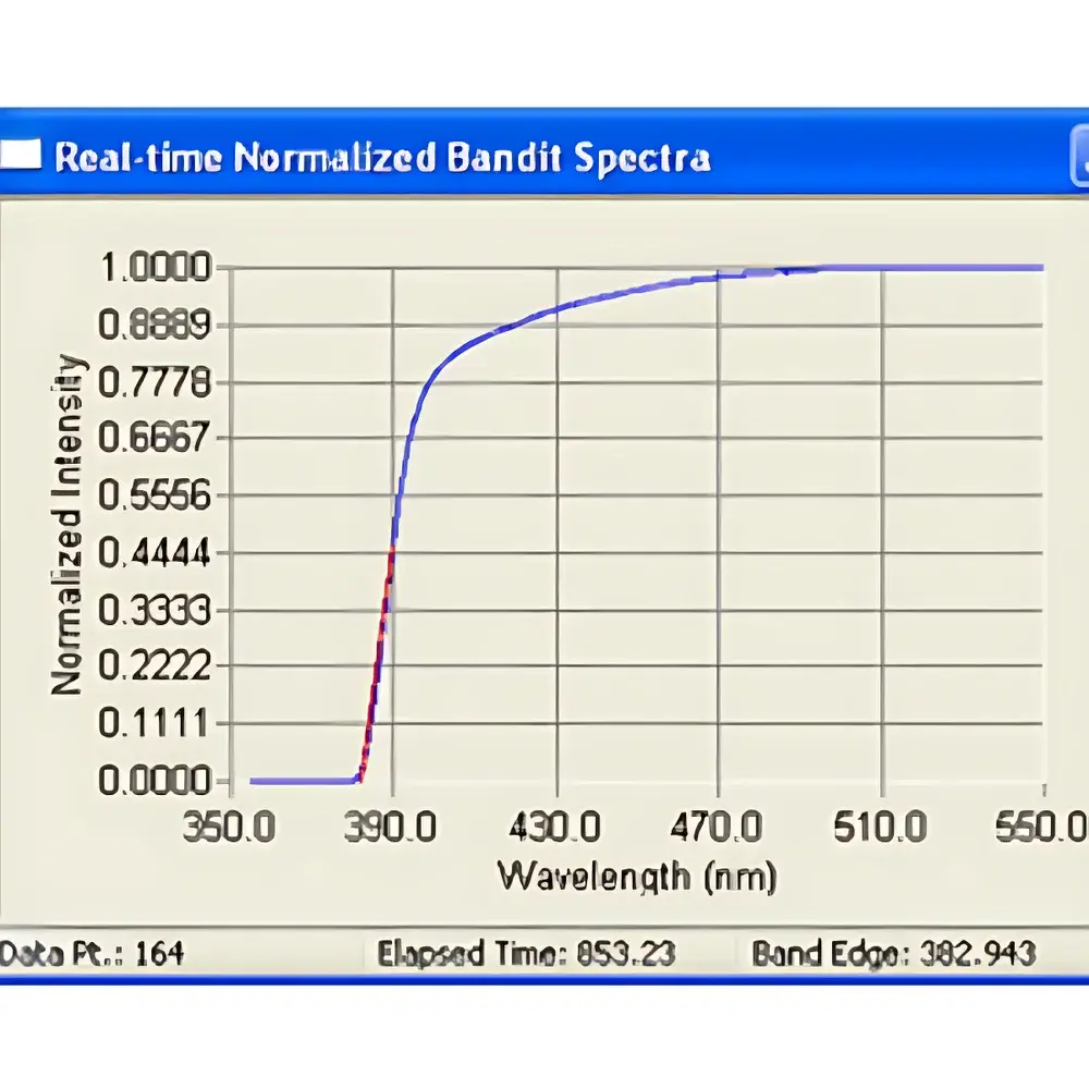
| Spectral Range | 350–1700 nm |
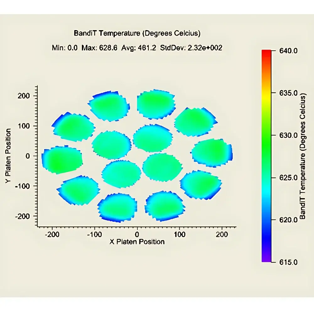
| Temperature Measurement Range | RT to 1300 °C |
| Temperature Resolution | 0.1 °C |
| Measurement Capabilities | Optical Band Gap, Spectral Absorption Profile, Film Thickness & Deposition Rate, Surface Roughness, In-Situ Thermal Monitoring |
Overview
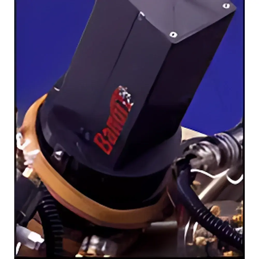
The BandiT PV Solar Thin-Film Photovoltaic Component In-Situ Characterization System is an advanced optical metrology platform engineered for real-time, non-contact analysis of thin-film photovoltaic (PV) materials during deposition and post-processing. Designed and manufactured by k-Space Associates (USA), the system integrates a high-stability AAA-class steady-state solar simulator with synchronized broadband spectroscopic reflectance/transmittance detection, thermal imaging, and surface topography sensing. Its core measurement principle relies on in-situ spectral ellipsometry combined with multi-wavelength photothermal reflectance and calibrated pyrometric temperature mapping—enabling simultaneous quantification of optical band gap (Eg), complex refractive index (n, k), film thickness, deposition rate, surface roughness (RMS), and substrate temperature across a broad spectral range (350–1700 nm). The system supports dynamic process monitoring under realistic thermal conditions—up to 1300 °C—with sub-degree thermal resolution (0.1 °C), making it particularly suitable for high-temperature vacuum deposition processes used in CIGS, CdTe, CIS, ZnO, GaN, SiC, and perovskite-based PV manufacturing.
Key Features
- AAA-class steady-state solar simulator compliant with IEC 60904-9:2020 and ASTM E927-19 standards for spectral match, spatial uniformity (>95%), and temporal stability (<2% variation over 1 h)
- Integrated broadband optical head covering UV-VIS-NIR (350–1700 nm) with high-resolution spectrometer (≤0.5 nm FWHM) and dual-channel detection for simultaneous reflectance/transmittance acquisition
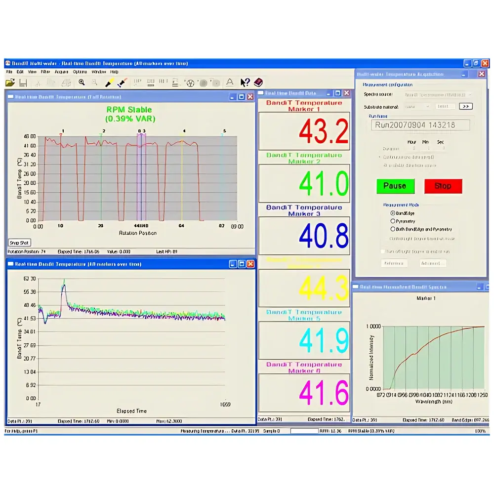
- In-situ temperature monitoring via calibrated two-color pyrometry with emissivity compensation; validated traceability to NIST-traceable blackbody sources
- Non-contact surface roughness estimation using angular-resolved scatterometry and statistical optical modeling (not AFM-equivalent, but correlated to RMS values within ±15% for films >50 nm)
- Real-time computation of Tauc plots for direct/indirect optical band gap determination, with automated baseline correction and derivative analysis
- Rugged industrial-grade enclosure rated IP54, compatible with integration into cluster tools, thermal evaporators, sputtering systems, and CVD reactors
Sample Compatibility & Compliance
The BandiT PV system accommodates substrates up to 300 mm in diameter and supports both rigid (glass, Si, sapphire, quartz) and flexible (stainless steel foil, polyimide) substrates. It is routinely deployed for characterization of chalcogenide absorbers (CdTe, CIGS, CZTS), transparent conductive oxides (ITO, AZO, ZnO), buffer layers (CdS, ZnS), and wide-bandgap semiconductors (GaN, SiC, SrTiO3). All optical calibration protocols adhere to ISO/IEC 17025 requirements when performed by k-Space-certified service engineers. The system’s data acquisition firmware supports audit trails and user access control, facilitating alignment with GLP and GMP documentation practices where required for R&D or pilot-line qualification.
Software & Data Management
Control and analysis are executed via k-Space’s proprietary BandiT Studio software (v5.2+), a Windows-based application supporting real-time plotting, batch processing, and export to CSV, HDF5, and MATLAB-compatible formats. The software includes built-in models for Tauc analysis, Bruggeman effective medium approximation (EMA), and Cauchy dispersion fitting. Data security features include optional 21 CFR Part 11-compliant electronic signatures, role-based permissions, and encrypted local storage. Raw spectral datasets are timestamped and annotated with environmental metadata (chamber pressure, gas flow, heater power), enabling full traceability from measurement to report generation.
Applications
- In-line optimization of sputter-deposited CdTe absorber layers through real-time band gap tracking during annealing
- Correlating ZnO:Al thickness growth rate with RF power and O2 partial pressure in reactive sputtering
- Monitoring interdiffusion-driven band gap grading in CIGS multilayer stacks during rapid thermal processing
- Quantifying surface roughness evolution during co-evaporation of CuInGaSe2 at >550 °C substrate temperatures
- Validating spectral absorption profiles of tandem perovskite/Si cells under simulated AM1.5G illumination
- Thermal stability assessment of metal-halide perovskites under sustained 85 °C illumination stress
FAQ
Does the BandiT PV support quantum efficiency (QE) or external quantum efficiency (EQE) measurements?
No—the BandiT PV is not configured for photocurrent-based QE/EQE. It measures optical properties only (absorption, reflectance, thickness, band gap). For combined optical + electrical characterization, k-Space recommends integration with third-party IV or IPCE systems via TTL synchronization.
Can the system operate inside a high-vacuum chamber?
Yes—optional UHV-compatible optical viewports and feedthroughs are available. Standard configuration is designed for atmospheric or low-pressure (<100 mTorr) environments; vacuum-rated variants require custom engineering review.
Is calibration traceable to national standards?
Yes—spectral radiance calibration is traceable to NIST SRM 2065 and 2066; temperature calibration is verified against NIST-traceable blackbody sources at three points (500 °C, 900 °C, 1200 °C) prior to shipment.
What substrates are incompatible with the system’s temperature measurement?
Highly reflective bare metals (e.g., uncoated Al or Cu below 400 °C) may yield inaccurate pyrometric readings due to variable emissivity; application of thin dielectric coatings or use of emissivity-matched reference samples is recommended.
Does the system meet FDA or ISO 13485 requirements for medical device manufacturing?
While not certified for medical device production, its data integrity architecture (audit trail, electronic signature, change control) aligns with foundational elements of ISO 13485:2016 Clause 7.5.2 and FDA 21 CFR Part 11 Subpart B for regulated R&D environments.


