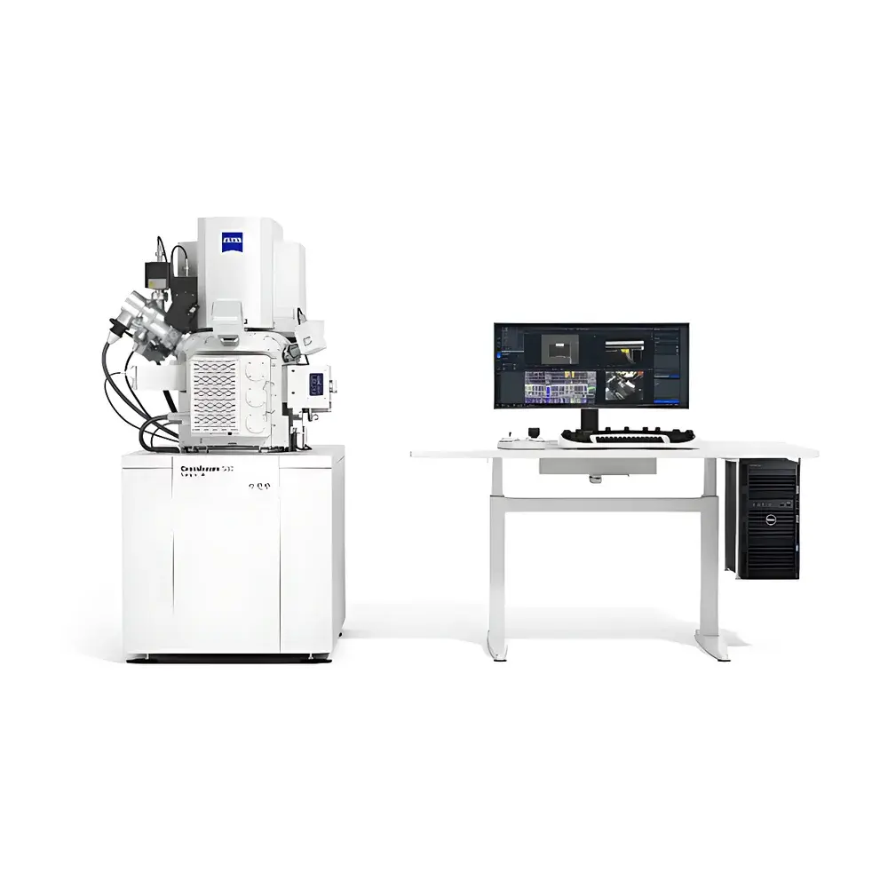
ZEISS Crossbeam 550 Samplefab Focused Ion Beam-Scanning Electron Microscope (FIB-SEM)
| Brand | ZEISS |
|---|---|
| Origin | Shanghai, China |
| Manufacturer Type | Authorized Distributor |
| Product Origin | Domestic (China) |
| Model | Crossbeam 550 Samplefab |
| Pricing | Upon Request |
Overview
The ZEISS Crossbeam 550 Samplefab is a high-precision dual-beam focused ion beam–scanning electron microscope (FIB-SEM) engineered specifically for transmission electron microscopy (TEM) specimen preparation in advanced semiconductor manufacturing and failure analysis laboratories. It integrates a gallium liquid metal ion source (LMIS) focused ion beam column with a field-emission scanning electron microscope (FE-SEM), enabling nanoscale imaging, precise site-specific milling, and reliable lift-out or pick-up workflows. The system operates on the principle of simultaneous or sequential electron- and ion-beam interaction with solid-state materials: the SEM provides real-time high-resolution topographic and compositional imaging (via secondary and backscattered electron detection), while the FIB enables sub-10 nm material removal, deposition, and cross-sectional milling under controlled vacuum conditions. Designed for 7 nm node and beyond process development, the Crossbeam 550 Samplefab supports deterministic, reproducible TEM lamella fabrication—critical for characterizing gate oxides, interconnect structures, and atomic-layer-deposited films.
Key Features
- Integrated dual-beam architecture with high-stability FE-SEM and high-current Ga⁺ FIB columns, optimized for low-k dielectric and ultra-thin Si channel milling.
- Automated TEM lamella preparation workflow including stage navigation, trench milling, under-cutting, and final thinning—reducing operator dependency and improving inter-lab reproducibility.
- Flexible lamella extraction protocols: in-situ lift-out using micro-manipulator-equipped Omniprobe™ or ex-situ pick-up with compatible TEM grid holders.
- Intuitive, industry-standard ZEISS SMART-SEM software interface with context-aware toolbars, scriptable automation (Python API), and integrated metrology tools for lamella thickness estimation.
- Enhanced beam stability and reduced drift via active vibration compensation and thermal management—essential for multi-hour serial sectioning and final thinning at <10 nm thickness.
- Dedicated Samplefab configuration includes STEM-in-SEM detector for inline bright-field/dark-field imaging during lamella transfer and quality verification prior to TEM insertion.
Sample Compatibility & Compliance
The Crossbeam 550 Samplefab accommodates standard 3-inch and 4-inch semiconductor wafers, diced dies on stubs, and packaged devices (with optional decapsulation modules). It supports conductive and non-conductive samples—including low-Z materials (SiO₂, SiNₓ), high-Z metallizations (Cu, Co, Ru), and emerging 2D materials (MoS₂, h-BN). All workflows comply with ISO/IEC 17025 requirements for testing laboratories and support audit-ready documentation per GLP and GMP environments. Software logs include full traceability of beam parameters (kV, pA, dwell time), stage coordinates, and user actions—aligned with FDA 21 CFR Part 11 electronic record and signature guidelines when configured with ZEISS Lab Management Suite.
Software & Data Management
ZEISS SMART-SEM v8.x provides unified control of both beams, automated recipe execution, and real-time image correlation between SEM and FIB frames. Data export conforms to TIFF, DM3, and HDF5 formats for downstream analysis in DigitalMicrograph®, Thermo Scientific Avizo®, or open-source platforms (e.g., TomoPy, HyperSpy). Integrated metadata embedding ensures FAIR (Findable, Accessible, Interoperable, Reusable) data principles. Optional ZEISS Connect enables secure remote monitoring, collaborative session sharing, and centralized instrument usage analytics across multi-site R&D facilities.
Applications
- Preparation of electron-transparent lamellae from FinFET, GAA (gate-all-around), and CFET (complementary FET) architectures for atomic-resolution TEM and EELS analysis.
- Failure isolation and root-cause analysis of opens, shorts, and electromigration-induced voids in backend-of-line (BEOL) interconnect stacks.
- In situ electrical probing via integrated nano-probe stations (optional) combined with FIB circuit edit capabilities.
- 3D reconstruction of device cross-sections through FIB-SEM serial sectioning (SBF-SEM) for process validation and defect tomography.
- Site-specific deposition of Pt/C-based protective layers and W-based conductive bridges during lift-out procedures.
FAQ
What TEM sample thickness can be achieved with the Crossbeam 550 Samplefab?
Final lamellae typically reach 50–100 nm thickness in the center region, with electron-transparent windows <30 nm achievable using low-voltage final polishing (2 kV, 50 pA) and cryo-stage options.
Is the system compatible with third-party TEM holders and transfer systems?
Yes—it supports standard Omniprobe™, Kleindiek MM3A, and Protochips Atmosphere™ holders, as well as JEOL and Thermo Fisher-compatible shuttle mechanisms.
Can the Crossbeam 550 Samplefab perform EBSD or EDS mapping during FIB milling?
EBSD indexing is supported post-milling on polished surfaces; EDS elemental mapping is available in SEM mode before, during, and after FIB processing—enabling composition-guided milling strategies.
Does ZEISS provide application support for semiconductor TEM workflow development?
Yes—ZEISS Application Scientists offer on-site workflow optimization, SOP development, and training aligned with JEDEC JESD22-A108 and ASTM F3061 standards for failure analysis.


