合肥科晶 Imported Fe₃O₄ Single-Crystal Substrate Wafers
| Brand | Hefei Kejing |
|---|---|
| Origin | USA |
| Supplier Type | Authorized Distributor |
| Import Status | Imported |
| Model | Fe₃O₄ Single Crystal Substrate |
| Crystal Orientation | <001>, <100>, <110>, <111> |
| Crystal Structure | Cubic, a = 8.40 Å |
| Density | 5.20 g/cm³ |
| Mohs Hardness | 5.5 |
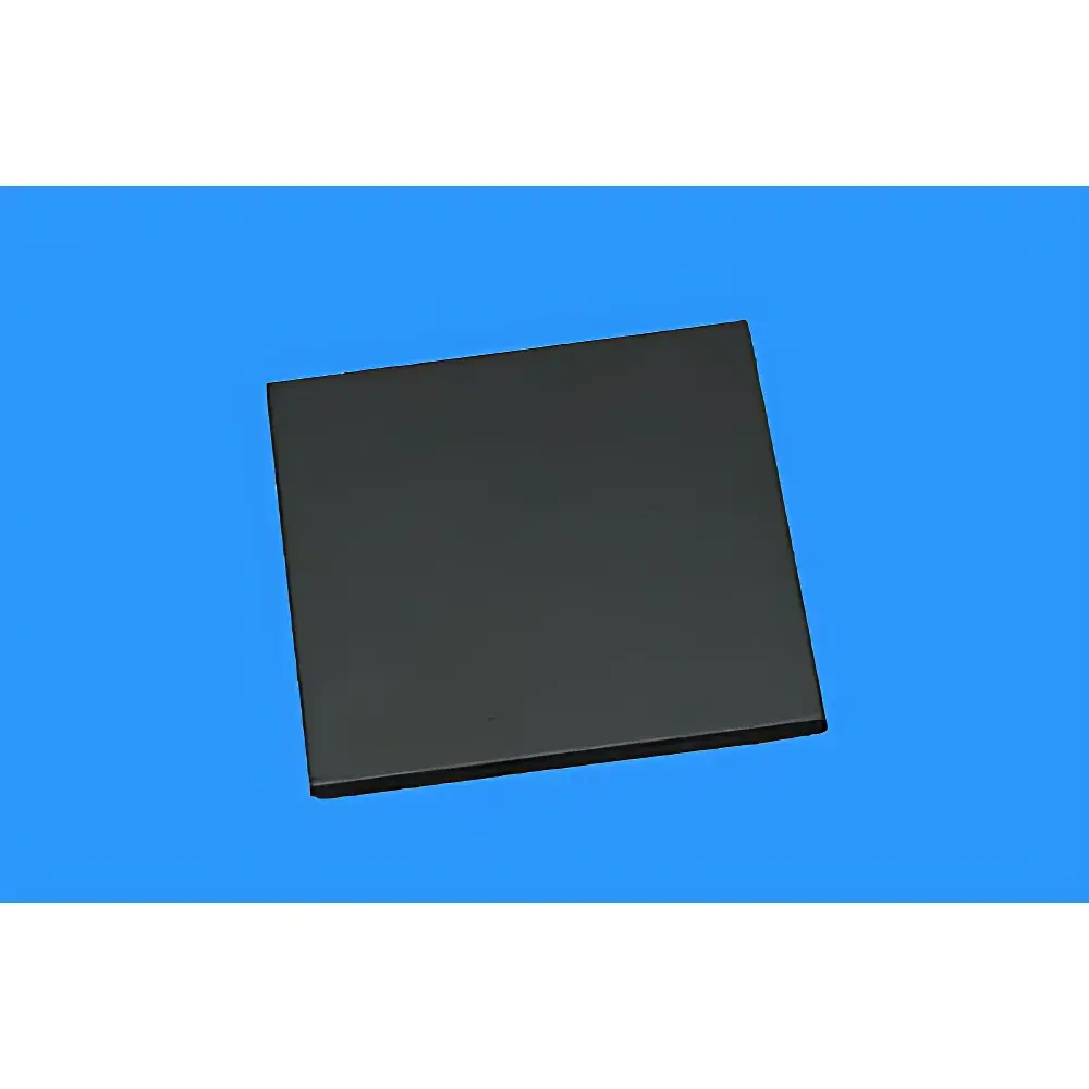
| Dimensions | 5 × 5 × 0.5 mm, 10 × 10 × 0.5 mm |
| Surface Finish | Single-Side Polished |
| Packaging | Class 1000 Cleanroom-Processed, Sealed in Class 100 Cleanroom Bags |
Overview
Hefei Kejing’s imported Fe₃O₄ (magnetite) single-crystal substrates are high-purity, orientation-controlled wafers engineered for advanced research in spintronics, magneto-optical spectroscopy, interfacial magnetism, and thin-film heteroepitaxy. Synthesized from naturally sourced, high-grade magnetite precursors and refined via flux-growth or vapor transport methods under controlled redox conditions, these substrates exhibit long-range crystalline order, low defect density, and stoichiometric Fe²⁺/Fe³⁺ ratio—critical for reproducible magnetic anisotropy and interfacial coupling studies. The cubic inverse spinel structure (space group Fd3̄m) enables well-defined surface termination and lattice-matching with perovskite oxides (e.g., LSMO, STO), making them indispensable for growth of epitaxial magnetic oxide films by pulsed laser deposition (PLD), molecular beam epitaxy (MBE), or sputtering.
Key Features
- Precisely oriented single-crystal surfaces: Available in , , , and orientations to support anisotropic property investigations and epitaxial strain engineering.
- High structural fidelity: Lattice parameter a = 8.40 Å confirmed by X-ray diffraction (XRD) rocking curve FWHM < 0.2°, indicating excellent crystallinity and minimal mosaic spread.
- Controlled surface quality: Single-side polished finish with RMS roughness < 0.3 nm (measured by atomic force microscopy), optimized for atomic-layer deposition and in situ surface characterization.
- Chemically stable and vacuum-compatible: Stable under UHV (<1×10⁻⁹ Torr) and moderate oxygen partial pressures; suitable for in situ annealing and surface-sensitive techniques including LEED, XPS, and STM.
- Rigorously clean handling: Processed and packaged in ISO Class 6 (1000) cleanroom environments; final sealing in ISO Class 5 (100) cleanroom bags ensures particulate contamination < 10 particles/m³ (≥0.5 µm).
Sample Compatibility & Compliance
These Fe₃O₄ substrates are compatible with standard semiconductor wafer handling tools, vacuum flange mounts (e.g., Kinematic, CF-35), and common substrate heaters (up to 400 °C in air, 300 °C in reducing atmospheres). They meet material traceability requirements for academic and industrial R&D labs operating under GLP-aligned workflows. While not certified to ASTM F1529 or SEMI standards (as they are research-grade substrates, not production wafers), dimensional tolerances conform to ±0.02 mm thickness control and ±0.1° orientation accuracy—verified per ASTM E975 for crystallographic orientation measurement. Batch-specific XRD, EDX, and AFM characterization reports are available upon request to support method validation and audit readiness.
Software & Data Management
As passive crystalline substrates, Fe₃O₄ wafers do not incorporate embedded electronics or firmware. However, their use is fully supported within standard materials characterization software ecosystems—including Bruker DIFFRAC.EVA (for XRD phase ID), Oxford Instruments AZtec (for elemental mapping), and Nanoscope Analysis (for AFM topography quantification). Each lot is assigned a unique traceability code enabling integration into laboratory information management systems (LIMS) for full sample lineage tracking. For labs adhering to FDA 21 CFR Part 11 or ISO/IEC 17025 requirements, documentation packages include raw test data, calibration certificates for metrology instruments used in QC, and cleanroom environmental logs.
Applications
- Epitaxial growth of complex oxide heterostructures for tunneling magnetoresistance (TMR) devices.
- Model system for studying Verwey transition dynamics (≈120 K) using transport, THz spectroscopy, and ultrafast optical probes.
- Substrate for van der Waals heterostructure assembly with 2D magnets (e.g., CrI₃, Fe₃GeTe₂).
- Reference material in magnetic force microscopy (MFM) and spin-polarized scanning tunneling microscopy (SP-STM) calibration protocols.
- Platform for electrochemical magnetization switching experiments in aqueous electrolytes.
FAQ
Are these Fe₃O₄ substrates conductive? How does conductivity affect device fabrication?
Yes—bulk Fe₃O₄ exhibits metallic conduction below the Verwey transition and semiconducting behavior above it. This intrinsic conductivity must be accounted for in gate dielectric design and contact engineering; insulating buffer layers (e.g., MgO, Al₂O₃) are commonly deposited prior to active channel formation.
Can I order custom orientations or thicknesses?
Custom orientations beyond standard offerings and thicknesses between 0.3–1.0 mm are available under minimum order quantities (MOQ: 10 wafers); lead time extends to 8–12 weeks for crystal growth and polishing cycles.
Is surface termination (Fe- vs O-terminated) specified?
Standard wafers are delivered as-received after chemical-mechanical polish and solvent rinse; surface termination is not stabilized or certified. In-situ surface preparation (e.g., Ar⁺ sputtering + annealing) is recommended prior to film growth to achieve reproducible terminations.
Do you provide XRD or Raman verification data with each shipment?
A representative batch certificate of analysis (CoA) including θ–2θ XRD scan, rocking curve, and Raman peak position (668 cm⁻¹ A₁g mode) is provided digitally with every order. Full spectral datasets are available upon request for method transfer or publication support.