WEP CVP21_ray Electrochemical Capacitance-Voltage Profiler
| Brand | WEP |
|---|---|
| Origin | Germany |
| Model | CVP21_ray |
| Instrument Type | Electrochemical Capacitance-Voltage Profiling System |
| Sample Compatibility | Semiconductor wafers (Si, Ge, SiC, GaN, InP, AlGaN, ZnO, CdTe, HgCdTe, etc.) |
| Carrier Concentration Range | 1×10¹¹ to 1×10²¹ cm⁻³ |
| Depth Resolution | Down to ≤1 nm |
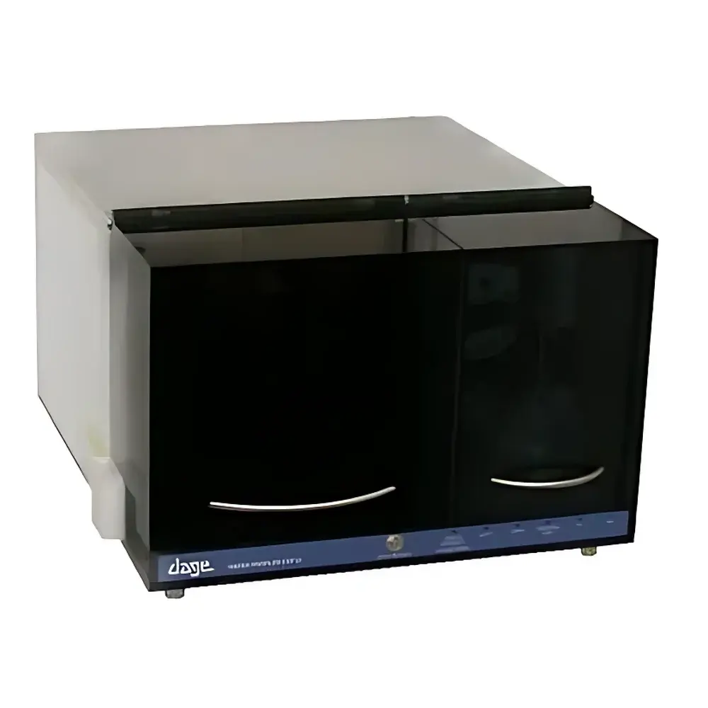
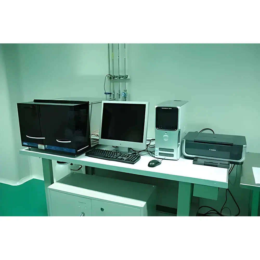
| System Architecture | Modular, cleanroom-compatible, fully automated electrochemical etching & CV scanning platform |
| Software Control | Integrated real-time etch monitoring, CV sweep automation, profile reconstruction, GLP-compliant data logging |
Overview
The WEP CVP21_ray is a fully automated electrochemical capacitance-voltage (ECV or CV) profiling system engineered for quantitative depth-resolved carrier concentration analysis in semiconductor materials. Based on the fundamental principle of electrochemical junction depletion—where controlled anodic etching removes material layer-by-layer while simultaneous high-frequency capacitance–voltage measurements track the evolving depletion width—the CVP21_ray reconstructs vertical dopant distribution profiles with sub-nanometer depth resolution. Unlike conventional secondary ion mass spectrometry (SIMS) or spreading resistance profiling (SRP), ECV provides direct, non-destructive (prior to etching), electrically relevant quantification of active dopant concentration (not total impurity), making it indispensable for process development and quality control in epitaxial growth, ion implantation, diffusion annealing, and heterostructure characterization. The system is widely deployed in photovoltaic R&D laboratories—including Fraunhofer ISE (Freiburg), ISFH (Hamelin), IMM (Nijmegen), and RWE Space Solar Power—and serves as a reference tool for silicon, III–V, III–nitride, II–VI, and wide-bandgap compound semiconductor development.
Key Features
- Modular, cleanroom-compatible architecture: Optically isolated measurement chamber, chemically segregated electrolyte handling module, and electrically shielded high-precision impedance interface ensure long-term stability and reproducibility.
- Sub-1 nm depth resolution: Achieved via synchronized potentiostatic etch control and 1 MHz small-signal CV acquisition, enabling reliable profiling of ultra-shallow junctions (<10 nm) and abrupt heterointerfaces.
- Automated, closed-loop profiling workflow: Software-directed electrolyte selection, electrode alignment, contact establishment, CV sweep sequencing, real-time etch rate monitoring, and automatic profile reconstruction eliminate operator-dependent variability.
- Broad material compatibility: Validated for Si, Ge, SiC, GaAs, InP, GaN, AlGaN, InGaN, AlInN, ZnO, CdTe, and HgCdTe; adaptable to novel substrates via custom electrolyte optimization and calibration protocols.
- High-fidelity circuit design: Low-noise transimpedance amplifiers, guarded guard-ring electrodes, and temperature-stabilized reference cells minimize parasitic capacitance and drift, supporting carrier concentration quantification from 1×10¹¹ cm⁻³ to 1×10²¹ cm⁻³.
Sample Compatibility & Compliance
The CVP21_ray accommodates wafer formats from 25 mm to 300 mm diameter, including patterned and textured surfaces common in PERC, TOPCon, and tandem solar cell fabrication. It supports both front-side and back-side contact configurations and integrates mechanical sample holders compatible with standard SEM/AFM stages for correlative metrology. All electrochemical modules comply with IEC 61000-6-3 (EMC emissions) and IEC 61010-1 (electrical safety for laboratory equipment). Data acquisition and reporting adhere to GLP principles: full audit trail, user authentication, electronic signatures, and timestamped raw CV/etch logs—fully compatible with FDA 21 CFR Part 11 requirements when deployed in regulated environments.
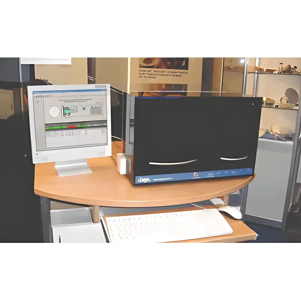
Software & Data Management
The proprietary CVP-Soft Suite (v5.x) provides intuitive GUI-based operation, scriptable batch processing, and ISO/IEC 17025-aligned uncertainty propagation modeling. Key modules include: (i) Electrolyte Database Manager (pre-loaded with >40 validated etchant systems for Si, GaN, InP, etc.), (ii) Real-Time Etch Monitor (graphical overlay of current transient vs. depth), (iii) CV Profile Reconstruction Engine (numerical solution of Poisson–Boltzmann boundary conditions), and (iv) Export Module supporting ASTM F1729-compliant .csv, .xlsx, and HDF5 formats. Raw data files retain full metadata (temperature, electrolyte lot ID, electrode history, calibration date), enabling traceable reprocessing and inter-laboratory comparison.
Applications
- Epitaxial layer validation: Quantifying dopant incorporation efficiency, uniformity, and interfacial segregation in MOCVD/MBE-grown SiGe, GaN-on-Si, or InP-based heterostructures.
- Ion implantation process control: Measuring activation efficiency, channeling effects, and post-anneal dopant redistribution in advanced CMOS and power device fabrication.
- Photovoltaic absorber characterization: Depth-resolved carrier profiling of CIGS, CdTe, perovskite/Si tandems, and passivating contacts (e.g., poly-Si/SiOx stacks).
- Wide-bandgap semiconductor R&D: Resolving Mg acceptor activation gradients in p-type GaN, dopant compensation in AlGaN barriers, and defect-related carrier trapping in SiC Schottky diodes.
- Failure analysis: Correlating electrical degradation in high-voltage devices with localized dopant pile-up or depletion at gate-edge interfaces.
FAQ
What semiconductor materials are supported out-of-the-box?
The system ships with validated electrolyte protocols for Si, Ge, GaAs, InP, GaN, and SiC. Custom protocols for emerging materials (e.g., β-Ga2O3, SnS, organic semiconductors) can be developed upon request.
Is cleanroom integration possible?
Yes—the CVP21_ray meets ISO Class 5 cleanroom requirements (particle count <3,520/m³ @ 0.5 µm) and features HEPA-filtered internal air circulation and static-dissipative housing.
How is measurement uncertainty quantified?
Uncertainty budgets follow GUM (JCGM 100:2008) methodology and include contributions from CV noise floor, etch rate variation, dielectric constant assumptions, and contact area estimation—reported per ASTM F1729 Annex A.
Can the system perform multi-point mapping?
Optional motorized X-Y-Z stage enables automated wafer mapping (up to 100 points/wafer) with positional repeatability ±1 µm and integrated focus tracking.
What software validation documentation is provided?
A complete IQ/OQ/PQ package—including installation checklist, operational verification scripts, performance qualification reports using NIST-traceable Si reference wafers—is supplied with each system.