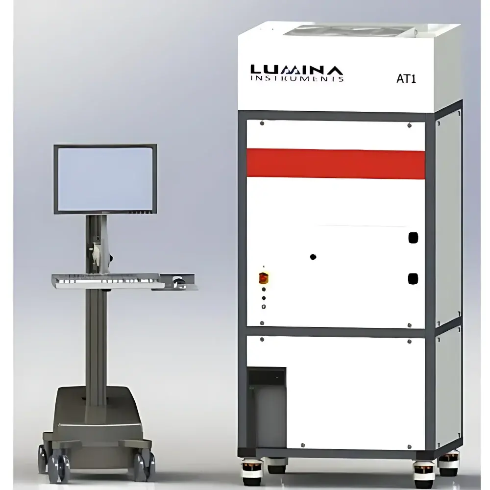
LUMINA AT1 Optical Surface Defect Analyzer
| Brand | LUMINA |
|---|---|
| Origin | USA |
| Model | AT1 |
| Type | Non-contact Profilometer / Surface Metrology System |
| Measurement Principle | Multi-modal Optical Scattering, Ellipsometry, Reflectometry, and Surface Slope Analysis |
| Sample Compatibility | Transparent (e.g., fused silica, sapphire, glass), semi-transparent (e.g., GaN, SiC), and opaque substrates (e.g., Si, GaAs, InP, metals) |
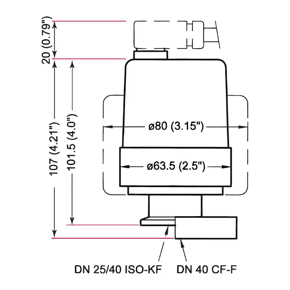
| Scan Area | Up to 300 × 300 mm |
| Wafer Handling | Supports 150 mm wafers (full-surface scan in ≤ 3 min), 50 × 50 mm samples in ≤ 30 s |
| Detection Sensitivity | Sub-nanometer vertical resolution for film thickness uniformity |
| Mechanical Architecture | Fixed-optics, non-rotating platform with high inertial damping |
| Regulatory Alignment | Designed for GLP/GMP-compliant environments |
Overview
The LUMINA AT1 Optical Surface Defect Analyzer is a high-precision, multi-modal surface metrology system engineered for comprehensive defect characterization and thin-film metrology on semiconductor wafers, optical substrates, and advanced electronic materials. Unlike conventional profilometers relying solely on mechanical stylus or single-mode optical interferometry, the AT1 integrates four complementary optical measurement channels—polarization-resolved ellipsometry, surface slope mapping, broadband reflectometry, and dark-field scattering—within a unified, non-contact platform. This architecture enables simultaneous acquisition of topographic, optical, and stress-related signatures across full wafers or large-area substrates (up to 300 × 300 mm), without physical contact, sample rotation, or vacuum requirements. Its design targets R&D laboratories and pilot-line fabs where rapid, repeatable, and physically non-invasive assessment of surface integrity, film uniformity, and subsurface anomalies is critical for process development, yield ramp-up, and failure root-cause analysis.
Key Features
- Multi-channel optical detection: Polarization channel for thin-film thickness, interfacial stress, and scratch-induced birefringence; slope channel for quantitative height/depth mapping of pits and bumps; reflectometry channel optimized for rough or diffusing surfaces (e.g., PR-coated wafers); dark-field channel for sub-100 nm particle and micro-scratch detection.
- Universal substrate compatibility: Validated on silicon, GaAs, InP, SiC, GaN, sapphire, fused quartz, display glass, and metal-coated optics—covering transparent, semi-transparent, and opaque material classes without hardware reconfiguration.
- High-throughput scanning: Full 150 mm wafer inspection completed in ≤ 180 seconds; localized 50 × 50 mm region-of-interest (ROI) analysis delivered in under 30 seconds—including image reconstruction, defect segmentation, and quantitative reporting.
- Robust mechanical platform: Vibration-damped granite base with air-isolation; fixed-optics configuration eliminates rotational inertia and stage-induced artifacts; accommodates non-circular, chipped, or warped samples (e.g., diced dies, prototype optics, AR/VR waveguides).
- Sub-nanometer vertical sensitivity: Achieved via phase-resolved ellipsometric reconstruction and calibrated slope integration—not dependent on laser wavelength alone—enabling reliable film-thickness uniformity mapping down to ±0.15 nm RMS across 100 mm fields.
Sample Compatibility & Compliance
The AT1 supports direct placement of bare and patterned wafers, polished optics, MEMS substrates, and lithography masks without clamping or vacuum chucking—minimizing risk of edge chipping or thermal distortion. It complies with ISO 25178-2 (surface texture parameters), ASTM E2926 (optical scatter-based defect classification), and SEMI F20 (wafer surface inspection standards). When deployed with optional LUMINA Validation Suite, the system meets analytical instrument qualification (AIQ) criteria for GxP environments, including documented IQ/OQ/PQ protocols, electronic signature support, and 21 CFR Part 11–compliant audit trails for all measurement events, parameter changes, and report generations.
Software & Data Management
The AT1 operates with LUMINA VisionPro™ v4.x—a modular, client-server application built on a PostgreSQL backend with role-based access control (RBAC). Core modules include DefectMap™ (automated classification using morphology + optical contrast heuristics), FilmUniformity™ (ellipsometric thickness grid analysis with statistical process control overlays), and SlopeTrace™ (gradient-based edge detection for CMP endpoint validation). All raw data (intensity maps, phase images, slope vectors) are stored in vendor-neutral HDF5 format with embedded metadata (timestamp, operator ID, calibration ID, environmental logs). Export options include CSV, TIFF, and industry-standard SEMI E142 (XML-based defect data exchange) for integration with factory MES and yield management systems.
Applications
- Pre- and post-CMP surface defect screening on Si, GaN, and sapphire wafers—identifying residual slurry particles, dishing, erosion, and subsurface microcracks.
- MOCVD and MBE epitaxial layer uniformity monitoring—quantifying thickness variation and stress gradients across 2–6 inch compound semiconductor wafers.
- Photolithography process control—measuring PR film thickness uniformity, edge bead removal efficacy, and developer-induced surface roughening.
- Clean process validation—comparing pre- and post-scan particle counts and size distributions following wet bench or plasma cleaning steps.
- AR/VR optical component metrology—characterizing waveguide surface flatness, anti-reflective coating homogeneity, and nanoimprint replication fidelity on curved or aspheric glass substrates.
- Mask shop quality assurance—detecting chrome defects, pellicle adhesion anomalies, and substrate-level haze on 4× reticles and EUV mask blanks.
FAQ
Does the AT1 require vacuum or inert gas purging for operation?
No. The system operates under ambient laboratory conditions with standard temperature and humidity control (20–25°C, 40–60% RH). No vacuum chamber or purge gas connections are needed.
Can the AT1 measure buried interface defects in multilayer stacks?
Yes—via polarization-sensitive ellipsometric depth profiling and coherent scattering modeling. It resolves interfacial voids, delamination precursors, and interdiffusion zones up to ~3 µm below the surface in transparent dielectrics.
Is calibration traceable to NIST or other national metrology institutes?
All optical path calibrations (slope, reflectance, ellipsometric offset) are performed using NIST-traceable step-height standards and certified reference mirrors. Certificate of Calibration includes uncertainty budgets per ISO/IEC 17025.
How is data security ensured during remote diagnostics or software updates?
Remote access requires dual-factor authentication and TLS 1.3–encrypted tunnels. Software updates are cryptographically signed and validated prior to installation; no telemetry or automatic cloud upload is enabled by default.
What maintenance schedule is recommended for long-term measurement stability?
Annual optical alignment verification and quarterly intensity normalization using onboard reference tiles. No consumables or user-serviceable optics are required; laser sources have >20,000-hour rated lifetime.