HORIBA JY In-situ Series Real-Time Spectroscopic Ellipsometer
| Brand | HORIBA |
|---|---|
| Origin | France |
| Model | In-situ Series |
| Application | In-line thin-film process monitoring during deposition and etching |
| Measurement Principle | Spectroscopic ellipsometry (SE) |
| Optical Configuration | Fiber-coupled, modular probe head design for integration into vacuum chambers or CVD/PVD/ALD tools |
| Spectral Range | Typically 190–1700 nm (configurable per system variant) |
| Spot Size | Adjustable, down to ~50 µm (dependent on optical interface and working distance) |
| Angle of Incidence | Fixed or motorized, commonly 65°–75° (customizable per integration requirement) |
| Measurement Speed | Up to 10 Hz spectral acquisition (full spectrum), sub-second single-wavelength monitoring |
| Single-Measurement Time | <100 ms (at fixed wavelength) |
| Sample Compatibility | Wafers up to 300 mm, flat or curved substrates, high-temperature or cryogenic environments (with optional thermal management) |
| Thickness Accuracy | ±0.1 nm (for SiO₂ on Si reference films, under controlled conditions) |
| Repeatability | <0.05 nm RMS over 24 h (thermal drift compensated) |
| n/k Determination Uncertainty | Δn < 0.002, Δk < 0.0005 (for transparent dielectrics) |
Overview
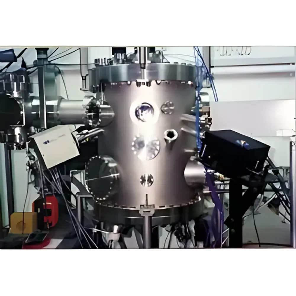
The HORIBA JY In-situ Series is a purpose-engineered spectroscopic ellipsometer designed for real-time, non-destructive characterization of thin-film growth and etch dynamics directly within industrial process tools. Operating on the physical principle of spectroscopic ellipsometry—measuring the change in polarization state (Ψ and Δ) of light reflected from a sample surface across a broad spectral range—the system delivers time-resolved data on film thickness, refractive index (n), and extinction coefficient (k). Unlike ex-situ benchtop ellipsometers, the In-situ Series features a fully fiber-optic architecture with compact, vacuum-compatible probe heads that integrate seamlessly into CVD, PVD, ALD, MBE, and plasma etch reactors. This enables continuous optical monitoring without breaking vacuum or interrupting process flow—critical for closed-loop process control, endpoint detection, and kinetic modeling of layer evolution.
Key Features
- Fiber-coupled optical design with separate illumination and collection paths, minimizing thermal crosstalk and enabling flexible routing through limited-access reactor ports.
- Modular probe head options: standard Brewster-angle configuration for high-sensitivity dielectric monitoring; variable-angle variants for anisotropic or multilayer stack analysis.
- Real-time spectral acquisition at up to 10 Hz, supporting both dynamic thickness tracking (single-wavelength mode) and full spectroscopic reconstruction (multi-wavelength mode) within the same measurement cycle.
- Embedded thermal stabilization and active drift compensation algorithms ensure long-term measurement stability under fluctuating chamber temperatures (±0.1 °C control).
- Robust mechanical housing rated for UHV (<1×10⁻⁹ mbar), bakeable to 150 °C, and compatible with corrosive process chemistries (e.g., Cl₂, F-based plasmas).
- Factory-calibrated using NIST-traceable Si/SiO₂ reference standards; supports user-defined calibration routines for proprietary substrate stacks.
Sample Compatibility & Compliance
The In-situ Series accommodates planar and slightly curved substrates ranging from 100 mm to 300 mm wafers, including silicon, sapphire, quartz, and compound semiconductor platforms. It operates reliably under high-radiation, high-temperature (up to 800 °C substrate temperature with appropriate window selection), and cryogenic conditions (down to 77 K). System compliance includes adherence to CE marking requirements for electromagnetic compatibility (EMC Directive 2014/30/EU) and low-voltage safety (LVD Directive 2014/35/EU). Data integrity protocols align with GLP and GMP expectations: audit trails, user access levels, electronic signatures, and raw-data export in HDF5 and ASCII formats satisfy FDA 21 CFR Part 11 readiness when deployed in regulated manufacturing environments.
Software & Data Management
Control and analysis are performed via HORIBA’s proprietary DeltaPsi² software platform—validated for ISO/IEC 17025-compliant laboratories. The software provides real-time visualization of Ψ(λ), Δ(λ), thickness vs. time, and n/k dispersion curves. Built-in regression engines support multi-layer optical modeling (Cauchy, Tauc-Lorentz, Cody-Lorentz parameterizations) with constraints for physical plausibility. All measurement sessions are timestamped, version-controlled, and archived with full metadata (process gas flows, power settings, temperature logs if interfaced). API access (Python/C++) enables integration with factory automation systems (SECS/GEM, OPC UA) for automated recipe-triggered measurements and SPC charting.
Applications
- Endpoint detection in plasma etching by tracking interference oscillations in Ψ(λ) during SiO₂ removal.
- Real-time monitoring of ALD Al₂O₃ nucleation kinetics and saturation behavior on functionalized surfaces.
- In-situ quantification of interfacial oxide growth during high-k gate stack deposition in CMOS fabrication.
- Dynamic characterization of perovskite film crystallization under thermal annealing in ambient or inert glovebox-integrated reactors.
- Monitoring compositional grading in ternary chalcogenide absorbers (e.g., CIGS) during co-evaporation.
FAQ
Can the In-situ Series be retrofitted into existing cluster tools?
Yes—its modular probe heads and fiber-optic interface allow integration via standard CF or KF flanges; HORIBA provides mechanical interface drawings and vacuum compatibility validation reports.
Does the system require periodic recalibration during extended runs?
No—built-in reference channel monitoring and thermal drift compensation eliminate need for manual recalibration over 72-hour continuous operation.
Is it possible to correlate ellipsometric data with process parameters such as RF power or gas flow?
Yes—DeltaPsi² supports analog/digital I/O synchronization and direct communication with PLCs or process controllers via Ethernet/IP or Modbus TCP.
What optical window materials are supported for different spectral ranges?
Fused silica (190–2500 nm), CaF₂ (150–900 nm), or sapphire (200–5500 nm) windows can be specified based on reactor environment and spectral requirements.
How is data security handled in shared fab environments?
Role-based access control (RBAC), encrypted local storage, and optional FIPS 140-2 compliant network encryption ensure compliance with semiconductor industry IT security policies.


