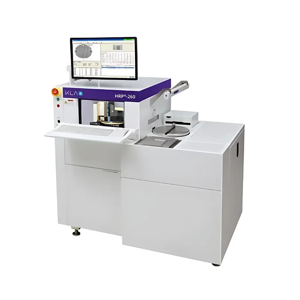
KLA HRP®-260 Contact Profilometer
| Brand | KLA |
|---|---|
| Origin | USA |
| Model | HRP®-260 |
| Measurement Principle | Stylus-based contact profilometry with dual-stage scanning (macro-stage + high-resolution piezo stage) |
| Scan Range | 200 mm (macro), 90 µm (high-res piezo) |
| Step Height Range | 0.1 nm to 327 µm |
| Normal Force Range | 0.03–50 mg |
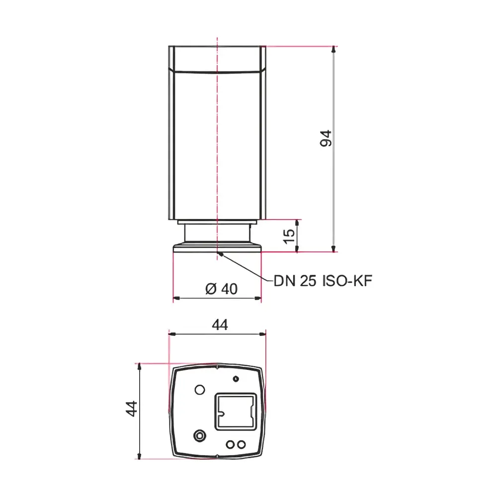
| Sample Diameter Support | 75–200 mm (opaque & transparent substrates) |
| Automation | Fully automated wafer handling, pattern recognition, SECS/GEM compliance |
| Software | Integrated metrology suite with ISO 4287/4288, ASME B46.1, and SEMI E10/E126 compliant analysis modules |
| Data Management | Audit-trail enabled, FDA 21 CFR Part 11 ready, GLP/GMP traceable reporting |
Overview
The KLA HRP®-260 Contact Profilometer is a production-proven, cassette-to-cassette metrology platform engineered for high-precision, high-throughput surface topography characterization in advanced semiconductor manufacturing and related precision industries. Unlike non-contact optical methods, the HRP®-260 employs a calibrated diamond-tipped stylus operating under closed-loop constant-force control—enabling direct physical measurement of surface elevation with sub-nanometer vertical resolution. Its dual-stage architecture integrates a long-range macro-scanning stage (up to 200 mm) with a high-resolution piezoelectric micro-stage (90 µm scan range), allowing seamless transition between full-wafer geometric inspection (warp, stress, shape) and localized nanoscale feature analysis (e.g., etch depth, lithographic line edge roughness, thin-film step coverage). This hybrid capability bridges the performance gap between conventional stylus profilometers and atomic force microscopes (AFM), delivering AFM-like lateral resolution without vacuum requirements or tip wear limitations inherent to scanning probe systems.
Key Features
- Dual-mode scanning architecture: Macro-stage for full-diameter wafer profiling (75–200 mm) and piezo-driven high-resolution stage for <90 µm scans at nanometer-level lateral fidelity
- UltraLite® sensor technology with real-time force feedback, maintaining consistent normal load between 0.03 mg and 50 mg across varying topography
- Integrated optical subsystem featuring coaxial low-magnification (1–5×) and high-magnification (20–100×) video imaging for rapid site navigation and feature targeting
- Automatic arc correction algorithm compensating for stylus trajectory curvature, eliminating systematic form error in long-range scans
- Full-wafer automated handling with robotic arm, compatible with both opaque (Si, SiC) and transparent (sapphire, glass) substrates
- SECS/GEM-compliant interface enabling integration into factory automation networks and MES systems
- Onboard leveling, filtering (Gaussian, Spline, Robust Gaussian), and reference-plane algorithms aligned with ISO 4287, ISO 4288, and ASME B46.1 standards
Sample Compatibility & Compliance
The HRP®-260 accommodates standard semiconductor wafers from 75 mm to 200 mm diameter—including silicon, gallium arsenide, silicon carbide, sapphire, and fused silica—without requiring custom fixtures or manual repositioning. Its force-controlled stylus system ensures reliable measurement on fragile, low-k dielectrics, photoresists, and MEMS structures where excessive loading could induce plastic deformation. All measurement workflows support audit-ready data logging per FDA 21 CFR Part 11 requirements, including electronic signatures, user access controls, and immutable change history. System validation documentation aligns with SEMI E10 (Definition of Terms Relating to Metrology) and SEMI E126 (Specification for Equipment Communication Standard—SECS Message Services), ensuring readiness for GMP/GLP-regulated environments.
Software & Data Management
The instrument operates via KLA’s proprietary Metrology Suite software—a Windows-based application designed for operator efficiency and engineering rigor. The GUI supports point-and-click measurement sequencing, template-driven recipe management, and batch processing of multi-site wafers. Analytical modules include comprehensive 2D/3D roughness parameter calculation (Ra, Rq, Rz, Sk, Spk, Smr), film stress derivation using Stoney’s equation, and 3D warp vector mapping. Raw profile data is stored in vendor-neutral ASCII formats (CSV, XYZ), while metadata—including calibration certificates, environmental logs, and operator credentials—is embedded in XML-based report packages. Data export supports LIMS integration, and all user actions are recorded in time-stamped, tamper-evident audit trails.
Applications
- Step height metrology for lithography, etch, and CMP processes—quantifying film thickness, trench depth, and overlay-induced topography
- Surface texture analysis per ISO 4287:2015, including amplitude, spacing, and hybrid parameters for functional surface assessment
- Wafer-level stress mapping of deposited films (e.g., SiNx, SiO2) using curvature-derived biaxial stress models
- 3D shape and warp evaluation for wafer bow, site flatness, and chuck-induced distortion
- Defect root-cause analysis via quantitative 3D morphology reconstruction of particles, scratches, and residues
- Cross-industry use in LED epitaxy (MQW layer uniformity), MEMS release etch verification, HDD media roughness, and automotive sensor wafer qualification
FAQ
What distinguishes the HRP®-260 from the P-260?
The HRP®-260 adds a high-resolution piezoelectric scanning stage to the base P-260 platform, enabling sub-10 nm lateral resolution over 90 µm fields—complementing the P-260’s 200 mm macro-scan capability.
Is the system qualified for use in ISO Class 5 cleanrooms?
Yes—the HRP®-260 meets SEMI S2 safety guidelines and can be configured with ESD-safe enclosures and HEPA-filtered internal airflow for Class 5 (ISO 14644-1) operation.
Does it support automated defect review workflows?
Yes—via integrated pattern recognition and coordinate transfer from inspection tools (e.g., KLA CIRCL, Applied Materials UVision), enabling precise re-measurement of flagged sites without manual intervention.
Can raw profile data be exported for third-party analysis?
Yes—ASCII (.csv, .txt) and industry-standard .xyz files are fully supported; metadata schemas comply with ASTM E2657 for interoperability with MATLAB, Python, and commercial metrology software.
What calibration standards are included?
NIST-traceable step height standards (100 nm–10 µm), roughness artifacts (Ra 0.02–2.0 µm), and certified flatness references are supplied with initial installation and annual service contracts.