BGA Solder Joint Inspection System – XG5010 X-ray Radiographic Inspection System
| Origin | Guangdong, China |
|---|---|
| Manufacturer Type | Authorized Distributor |
| Origin Category | Domestic (PRC) |
| Model | XG5010 |
| Price Range | USD 28,000 – 70,000 |
Overview
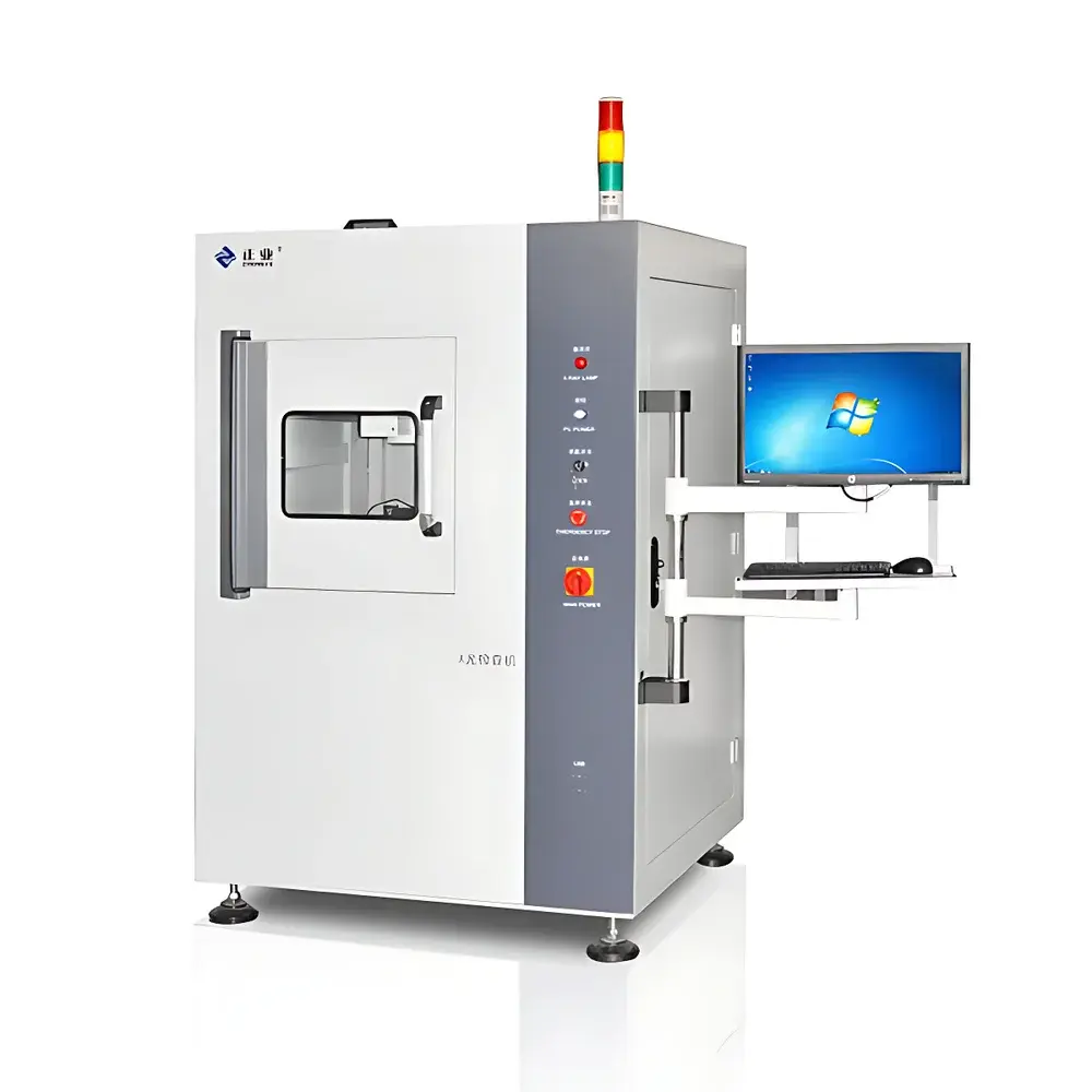
The XG5010 BGA Solder Joint Inspection System is a high-resolution, cabinet-type X-ray radiographic inspection platform engineered for non-destructive evaluation of ball grid array (BGA), chip-scale package (CSP), and other fine-pitch area-array interconnects in electronics manufacturing. It operates on the principle of differential X-ray attenuation: as a microfocus X-ray beam (≤5 µm focal spot size) penetrates the test sample, variations in material density and thickness generate contrast in the transmitted radiation, which is captured by a high-sensitivity flat-panel detector and enhanced via real-time digital image processing. This enables quantitative assessment of solder joint integrity—including voiding, bridging, insufficient wetting, head-in-pillow (HIP), and missing or misaligned balls—without disassembly or physical contact. Designed for integration into SMT line monitoring, incoming component qualification, post-reflow verification, and rework validation workflows, the XG5010 complies with IPC-A-610 and J-STD-001 requirements for solder joint acceptability criteria.
Key Features
- Microfocus sealed-tube X-ray source (≤5 µm focal spot) delivering stable, low-noise beam output for high-contrast imaging of sub-100 µm solder joints
- 16-bit dynamic range flat-panel detector with 1024 × 1024 pixel resolution and real-time frame averaging to suppress quantum noise
- Motorized XYZ stage with programmable precision positioning (±1 µm repeatability) and tilt/rotation capability for multi-angle oblique viewing
- Integrated image enhancement suite including edge sharpening, contrast normalization, false-color mapping, and void segmentation algorithms
- Lead-shielded cabinet conforming to IEC 61331-1:2014 radiation safety standards; interlocked door system with automatic beam cutoff
- CE-marked electrical architecture compliant with EN 61000-6-2 (EMC immunity) and EN 61000-6-4 (EMC emission) directives
Sample Compatibility & Compliance
The XG5010 accommodates PCB assemblies up to 400 mm × 300 mm in footprint and 50 mm in height, supporting single- and double-sided boards with BGA pitches down to 0.3 mm. It is validated for use with leaded (SnPb) and lead-free (SAC305, SAC405) solder alloys, ceramic and plastic laminate substrates, and stacked-die packages. All measurement protocols align with IPC-A-610 Class 2 and Class 3 visual acceptance criteria. Image acquisition metadata—including kV, µA, exposure time, magnification factor, and detector gain—is automatically embedded in DICOM-compliant files to support traceability under ISO 9001 and IATF 16949 quality management systems.
Software & Data Management
Equipped with proprietary XRayVision™ inspection software, the XG5010 provides calibrated void analysis (void area %, maximum void diameter, void distribution histogram), automated defect classification (via rule-based pattern matching), and batch report generation in PDF/XLS formats. Audit trails record operator ID, timestamp, parameter settings, and image annotations—fully compliant with FDA 21 CFR Part 11 requirements for electronic records and signatures when configured with user authentication and role-based access control. Raw images and processed data are exportable in TIFF, PNG, and DICOM formats for integration into MES or PLM platforms.
Applications
- Inline process verification during SMT reflow profiling and post-reflow AOI correlation
- Incoming inspection of BGA components prior to placement to detect pre-existing voids or coplanarity defects
- Fault isolation in field-failure analysis (FFA) involving thermal cycling-induced solder fatigue or intermetallic fracture
- Process development support for optimizing reflow profiles, solder paste volume, and stencil aperture design
- Qualification of BGA rework stations by validating solder joint morphology before and after reballing
- Support for automotive electronics (AEC-Q200 qualified assemblies) and medical device PCBs requiring full inspection traceability
FAQ
What is the minimum detectable void size under standard operating conditions?
Under nominal 10× geometric magnification and 90 kV tube voltage, the system reliably resolves voids ≥25 µm in diameter with ≥95% detection probability at 3σ confidence level.
Does the XG5010 support automated pass/fail decision logic based on IPC void limits?
Yes—user-defined void thresholds (e.g., max 25% void area per joint per IPC-A-610 Section 10.2.3) can be programmed into inspection recipes, triggering color-coded overlays and binary pass/fail flags in reports.
Is remote diagnostics and software update capability available?
The system includes secure TLS-enabled remote maintenance port; firmware and application updates are delivered via authenticated HTTPS download with SHA-256 signature verification.
Can the XG5010 inspect 3D-stacked packages such as PoP (Package-on-Package)?
Yes—using multi-angle tomographic acquisition mode (up to 180° rotation), the system reconstructs layered solder interfaces in PoP configurations, enabling independent evaluation of top and bottom BGA interconnects.
What calibration documentation is provided with the instrument?
Each unit ships with NIST-traceable X-ray output calibration certificate (kV, µA, dose rate), spatial resolution test chart verification report (per ASTM E2737-18), and annual performance verification checklist aligned with ISO/IEC 17025 accredited lab procedures.
")


