Zhengye XK32A Automated Line Width Measurement System
| Brand | Zhengye |
|---|---|
| Origin | Guangdong, China |
| Manufacturer Type | Direct Manufacturer |
| Region of Origin | Domestic (China) |
| Model | XK32A |
| Pricing | Upon Request |
Overview
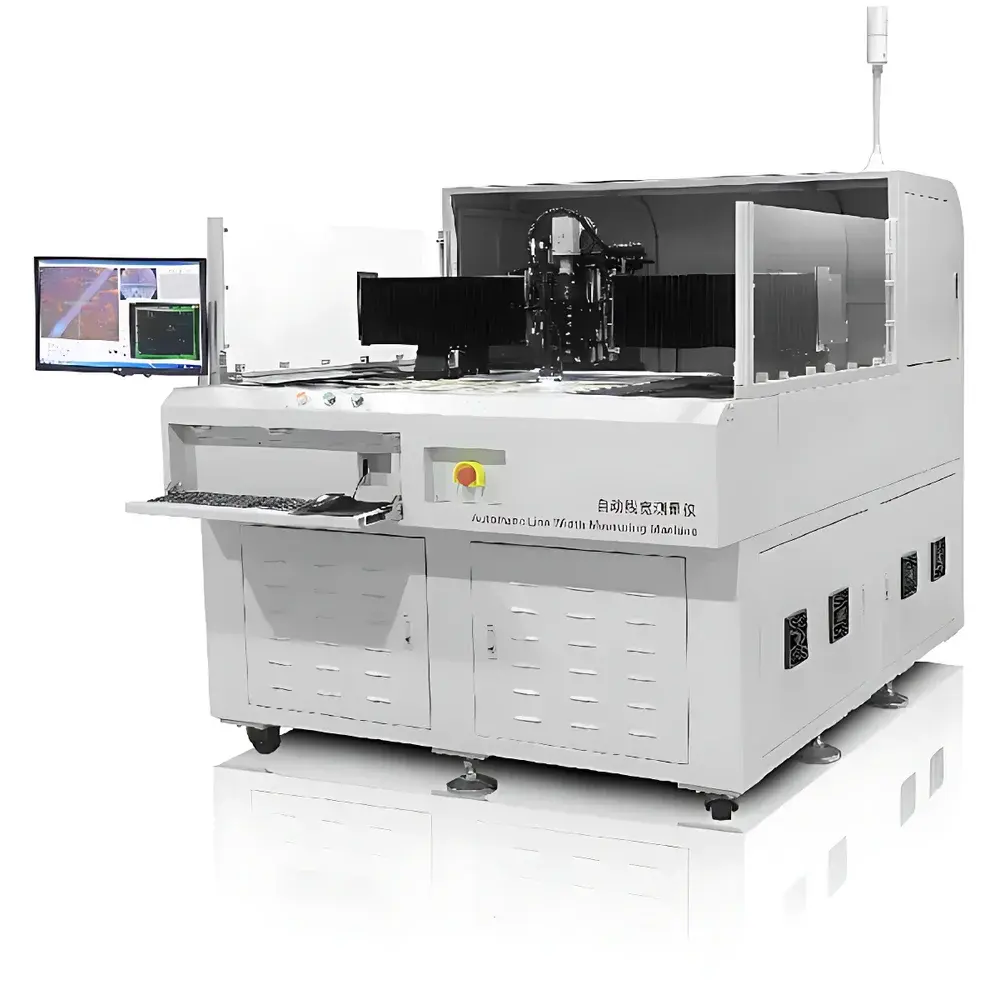
The Zhengye XK32A Automated Line Width Measurement System is an industrial-grade optical metrology instrument engineered for high-precision, non-contact dimensional inspection of printed circuit board (PCB) features. It operates on the principle of high-resolution digital imaging combined with calibrated machine vision algorithms to quantify critical geometric parameters—including line width (top and bottom profiles), line spacing (pitch), circular via diameters, and gold finger trace widths—on both inner and outer layer PCB substrates after developing and etching, but prior to solder mask application. Designed specifically for 5G infrastructure PCBs and advanced HDI (High-Density Interconnect) boards, the XK32A delivers repeatable sub-micron measurement capability within its field of view, supporting stringent IPC-6012 and IPC-A-600 compliance verification workflows in production environments.
Key Features
- Fourth-generation platform with upgraded optical imaging subsystem: includes high-stability coaxial LED illumination, telecentric lens assembly, and 5-megapixel progressive-scan CMOS camera optimized for edge contrast enhancement and minimal parallax error.
- Automated measurement engine with real-time image acquisition and batch processing: supports concurrent analysis of multiple features across a single frame, including asymmetric line profiles (top vs. bottom width), center-to-center spacing, and circular feature diameter deviation.
- Dedicated PCB metrology software with configurable tolerance mapping: enables user-defined GD&T (Geometric Dimensioning and Tolerancing) rules per layer, automatic pass/fail classification per measurement point, and statistical process control (SPC) data export (X-bar/R, Cp/Cpk).
- Robust mechanical architecture: precision-ground granite base, motorized Z-axis focus adjustment, and programmable XY stage with ±0.5 µm repeatability—designed for integration into inline or offline SMT/PCB fabrication lines.
- Compliance-ready audit trail functionality: full measurement log recording (timestamp, operator ID, image thumbnail, raw pixel coordinates, calibration status) aligned with GLP/GMP documentation requirements and internal quality system audits.
Sample Compatibility & Compliance
The XK32A accommodates standard rigid and flex-rigid PCB panels up to 610 mm × 457 mm (24″ × 18″), with thickness ranging from 0.05 mm to 3.2 mm. It supports copper-clad laminates (FR-4, polyimide, Rogers), solder mask–free substrates, and electroplated gold or ENIG-finished surfaces. Measurement traceability is maintained through NIST-traceable calibration artifacts and annual verification protocols compliant with ISO/IEC 17025–accredited laboratory practices. The system meets functional requirements referenced in IPC-TM-650 Section 2.2.13 (Optical Measurement of Conductor Dimensions) and supports documentation formats required for AS9100 and IATF 16949 quality management systems.
Software & Data Management
The embedded Zhengye Vision Metrology Suite (v4.2+) provides intuitive GUI-based measurement setup, automated feature recognition (via edge detection and Hough transform algorithms), and customizable reporting templates (PDF, CSV, XLSX). All measurement sessions are logged with immutable metadata—including camera exposure settings, lens magnification factor, stage position, and software version—ensuring full 21 CFR Part 11–compatible electronic record integrity when configured with user authentication and digital signature modules. Raw image archives and processed result sets can be exported to enterprise MES or QMS platforms via secure FTP or OPC UA interfaces.
Applications
- Pre-solder mask inspection of fine-pitch traces (≤50 µm line/space) in 5G mmWave RF layers and high-speed SerDes routing stacks.
- Process validation for etch uniformity and sidewall profile consistency across multi-layer sequential build-up (SBU) PCBs.
- First-article inspection (FAI) and periodic capability studies for Class 3 aerospace and medical electronics assemblies per IPC-A-610.
- Root cause analysis of open-circuit defects linked to under-etching or over-etching via comparative line width trend analysis across panel zones.
- Supplier qualification support for bare board vendors requiring objective, operator-independent dimensional verification reports.
FAQ
What is the minimum measurable line width supported by the XK32A?
The system achieves reliable detection and quantification of conductor features down to 25 µm under optimal lighting and focus conditions, subject to surface finish and contrast ratio.
Does the XK32A support automatic defect marking on the image?
Yes—measurement outliers exceeding user-defined tolerances are highlighted with color-coded overlays and annotated with deviation values directly on the captured image.
Can the system integrate with factory automation protocols?
It supports Modbus TCP and Ethernet/IP for basic I/O handshake; full SECS/GEM integration requires optional middleware configuration.
Is calibration certification included with delivery?
Each unit ships with a factory calibration report referencing traceable standards; on-site ISO/IEC 17025 calibration services are available upon request.
What operating system is required for the host PC?
Windows 10 Pro (64-bit) or Windows 11 IoT Enterprise, with dedicated GPU support recommended for real-time image rendering at full sensor resolution.


