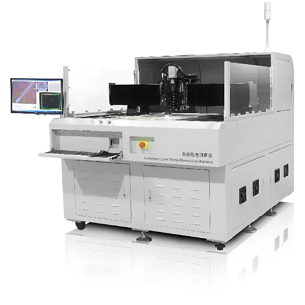
Zhengye XK32A Automated In-Line PCB Trace Width & Spacing Measurement System
| Brand | Zhengye |
|---|---|
| Origin | Guangdong, China |
| Manufacturer Type | OEM/ODM Manufacturer |
| Country of Origin | China |
| Model | XK32A |
| Pricing | Upon Request |
Overview
The Zhengye XK32A Automated In-Line PCB Trace Width & Spacing Measurement System is an industrial-grade vision-based metrology platform engineered for non-contact, high-throughput inspection of printed circuit board (PCB) conductor features during mid- to late-stage fabrication. It operates on the principle of high-resolution optical imaging combined with sub-pixel edge detection algorithms, enabling precise quantification of critical dimensional parameters—including trace upper width, lower width, line-to-line spacing, circular via diameters, and gold finger linewidth—on both inner and outer layer panels post-development and pre-solder mask application. Designed specifically for 5G RF multilayer boards, HDI substrates, and advanced rigid-flex assemblies, the XK32A integrates into automated production lines or standalone QC stations, delivering real-time pass/fail decisions against user-defined GD&T tolerances per IPC-6012, IPC-A-600, and IPC-2221 standards.
Key Features
- True in-line compatibility with conveyor-integrated mounting and programmable trigger synchronization for continuous panel scanning at speeds up to 1.2 m/min
- High-stability coaxial illumination system with adjustable LED ring light and telecentric lens assembly to minimize perspective distortion and shadow artifacts
- 12-megapixel global-shutter CMOS sensor with 2.2 µm pixel pitch, supporting configurable field-of-view (FOV) from 8 mm × 6 mm to 25 mm × 18.75 mm
- Dual-edge detection engine calibrated for copper-clad FR-4, polyimide, and ceramic substrates—capable of resolving linewidths down to 25 µm with ±0.5 µm repeatability (3σ)
- Real-time measurement feedback via Ethernet/IP or Modbus TCP, compatible with MES/SCADA integration for SPC charting and OEE tracking
- Self-diagnostic calibration routine with NIST-traceable step gauge reference and automated focus drift compensation
Sample Compatibility & Compliance
The XK32A accommodates standard PCB panel sizes from 18″ × 24″ (457 mm × 610 mm) up to 24″ × 30″ (610 mm × 762 mm), with thickness range 0.05–3.2 mm and surface finish compatibility spanning bare copper, ENIG, ENEPIG, immersion tin, and OSP. All measurement algorithms adhere to ISO/IEC 17025-accredited validation protocols; software audit trails comply with FDA 21 CFR Part 11 requirements for electronic records and signatures when configured with user authentication and role-based access control. System validation documentation supports GLP/GMP environments and satisfies internal quality audits aligned with IATF 16949 and ISO 9001:2015.
Software & Data Management
Powered by Zhengye VisionMaster v4.2, the embedded measurement suite provides intuitive GUI-driven setup of multi-zone inspection plans, tolerance mapping per feature class, and statistical process monitoring dashboards. Raw image archives, measurement logs, and SPC data are stored in SQLite3 databases with optional encryption and scheduled export to network shares or cloud storage (AWS S3, Azure Blob). The software includes full revision history, change log tracking, and automated report generation in PDF/XLSX formats compliant with IPC-7351B naming conventions. Optional API modules support custom integration with factory ERP systems (SAP, Oracle) and AI-based defect classification engines via RESTful webhooks.
Applications
- Final verification of etch uniformity on HDI microvias and fine-pitch traces prior to solder mask lamination
- Statistical analysis of line width variation across panel zones to identify plating bath drift or photolithography alignment errors
- Process capability assessment (Cp/Cpk) for 5G mmWave antenna arrays requiring ≤±3 µm line width control
- Root cause analysis of open-circuit failures linked to under-etching or sidewall taper anomalies
- Supplier qualification testing per IPC-6012 Class 3 requirements for aerospace and medical electronics
FAQ
What is the minimum measurable line width and spacing supported by the XK32A?
The system achieves reliable detection of conductors as narrow as 25 µm with a measurement resolution of 0.1 µm under optimal lighting and focus conditions.
Does the XK32A support automatic calibration without manual intervention?
Yes—it performs daily self-calibration using a motorized reference stage and certified step gauge; full system validation requires quarterly third-party verification.
Can the software generate SPC charts compliant with ISO 7870-2?
Yes—built-in X-bar/R and Cpk calculators export time-series data directly to Minitab- or JMP-compatible CSV formats.
Is remote diagnostics and firmware update capability available?
Yes—secure SSH-enabled remote access allows authorized engineers to monitor system health, retrieve logs, and deploy OTA updates via HTTPS.
How does the XK32A handle warped or bowed panels during measurement?
Integrated laser triangulation height mapping corrects Z-axis positional error in real time, ensuring consistent focus plane alignment across ±2 mm bow deviation.