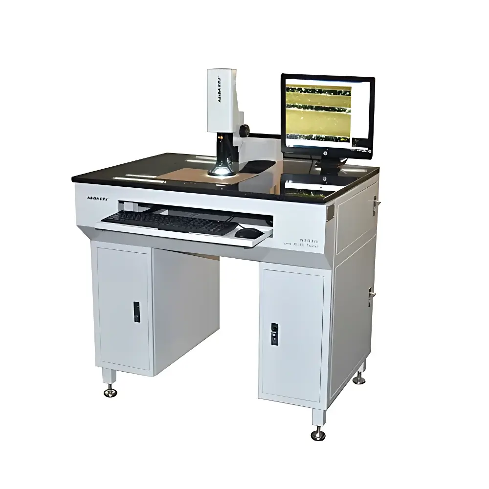
Zhengye XK25 PCB Line Width Measurement System
| Brand | Zhengye |
|---|---|
| Origin | Guangdong, China |
| Manufacturer Type | OEM/ODM Manufacturer |
| Country of Origin | China |
| Model | XK25 |
| Pricing | Available Upon Request |
| Measurement Accuracy | ±1 µm |
| Pixel Resolution | 0.4–2.7 µm/pixel |
| Total Optical Magnification | 70×–450× |
| Objective Magnification | 1.4×–9× (Continuously Adjustable) |
| Max. PCB Width | ≤760 mm |
| Field of View | 0.53×0.4 mm – 3.3×2.5 mm |
| Measurable Line Width Range | 20–1200 µm |
| Dimensions (W×D×H, excl. PC) | 960×780×1280 mm |
| Weight | 145 kg |
Overview
The Zhengye XK25 PCB Line Width Measurement System is a high-precision optical metrology instrument engineered for non-contact, two-dimensional dimensional analysis of printed circuit board (PCB) features. It operates on the principle of digital image acquisition combined with sub-pixel edge detection algorithms and calibrated optical magnification, enabling traceable, repeatable quantification of critical geometric parameters—including conductor line width (top and bottom), line-to-line spacing, pad-to-trace clearance, hole-to-edge distance, circular/oval via diameters, and curved feature radii. Designed specifically for inline or offline quality assurance in PCB fabrication facilities, the system supports measurement tasks performed after etching and prior to solder mask application—ensuring compliance with IPC-6012, IPC-A-600, and J-STD-003 requirements for conductor geometry verification. Its modular architecture integrates a motorized zoom lens, high-resolution monochrome CMOS sensor, coaxial red LED illumination for rapid feature localization, and precision mechanical stage capable of stable positioning across large-format substrates up to 760 mm wide.
Key Features
- Sub-pixel edge detection algorithm delivering measurement repeatability within ±1 µm across the full 20–1200 µm line width range
- Continuously adjustable optical magnification (1.4×–9×) paired with digital zoom to achieve total system magnification from 70× to 450×, optimized for both macro-feature survey and micro-feature resolution
- Calibrated pixel pitch ranging from 0.4 µm to 2.7 µm per pixel—configurable based on objective selection and field-of-view requirements
- Integrated red LED crosshair projection for intuitive operator alignment and rapid ROI (Region of Interest) targeting
- Automated edge-finding routines compliant with ISO 10360-8 for coordinate measuring machine (CMM)-class dimensional metrology workflows
- Robust mechanical design with granite base and vibration-damped stage; overall footprint 960 × 780 × 1280 mm (excl. host PC); unit mass 145 kg for thermal and mechanical stability
Sample Compatibility & Compliance
The XK25 accommodates rigid and flexible PCBs, IC substrates, thin-film transistor (TFT) arrays, and LCD panel photomasks. It accepts boards up to 760 mm in width and supports FOVs from 0.53 × 0.4 mm (high-magnification mode) to 3.3 × 2.5 mm (wide-field survey mode). All measurements are traceable to NIST-calibrated standards via factory-certified lens calibration certificates. The system meets functional requirements outlined in IPC-TM-650 2.2.15 (Optical Microscopy Measurement Procedures) and supports documentation protocols aligned with ISO 9001, IATF 16949, and FDA 21 CFR Part 11 when integrated with validated software modules (audit trail, electronic signature, data integrity controls).
Software & Data Management
The bundled measurement software provides real-time image capture, multi-point calibration, batch measurement scripting, and SPC (Statistical Process Control) analytics—including X̄-R charts, Cp/Cpk calculation, histogram generation, and out-of-spec alerting. Raw images and coordinate datasets are stored in vendor-neutral TIFF and CSV formats. Optional GLP/GMP-compliant configuration includes user access levels, change logs, electronic signatures, and 21 CFR Part 11 audit trails—enabling use in regulated electronics manufacturing environments subject to third-party quality audits.
Applications
- Verification of etch uniformity and undercut profiles on inner/outer layer PCBs pre-solder mask
- Quantitative assessment of fine-pitch trace geometry in HDI and mSAP processes
- Dimensional validation of BGA substrate traces, fan-out wafer-level packaging (FOWLP) redistribution layers, and silicon interposers
- Line width and space metrology for TFT-LCD array substrates and OLED backplane patterning
- Failure analysis support for root cause identification in short-circuit or open-circuit defects linked to dimensional deviations
- Process capability studies supporting APQP and PPAP documentation for Tier-1 automotive electronics suppliers
FAQ
Is the XK25 compatible with automated factory data systems (e.g., MES or SECS/GEM)?
Yes—via optional OPC UA or TCP/IP API integration, enabling bidirectional communication with manufacturing execution systems for automated job dispatch and result upload.
Does the system support measurement of blind vias and microvias?
Yes—using top-surface imaging and calibrated depth-of-field optimization, the XK25 measures diameter and annular ring width of blind/microvias with ≥3 µm lateral resolution under optimal lighting conditions.
Can measurement data be exported in formats acceptable for external SPC platforms?
Yes—CSV, XLSX, and XML exports include metadata (timestamp, operator ID, calibration ID, measurement uncertainty estimate) and conform to MSA AIAG 4th Edition formatting conventions.
What maintenance is required to sustain measurement accuracy over time?
Annual recalibration against NIST-traceable step gauges and lens distortion verification is recommended; daily warm-up and focus validation using certified reference slides ensure ongoing performance consistency.