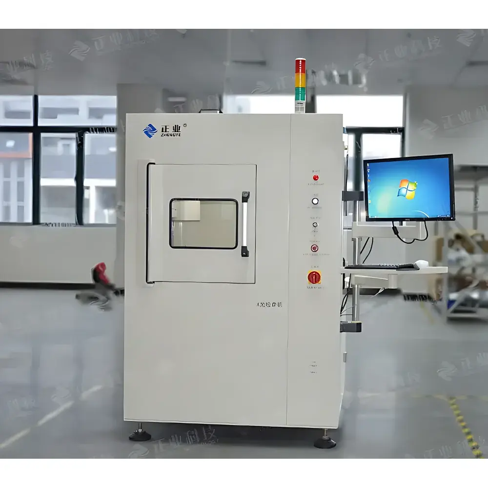
Zhengye X-ray Inspection System for Non-destructive Solder Joint Analysis in Semiconductor Packages
| Brand | Zhengye |
|---|---|
| Origin | Guangdong, China |
| Manufacturer Type | OEM/ODM Manufacturer |
| Regional Classification | Domestic (PRC) |
| Model | ChipInspection-XR250 |
| Pricing | Available Upon Request |
Overview
The Zhengye ChipInspection-XR250 is a high-precision, industrial-grade X-ray inspection system engineered specifically for non-destructive evaluation of solder joints within semiconductor packages and microelectronic assemblies. Utilizing real-time transmission radiography based on sealed-tube microfocus X-ray technology (typically 90–130 kV, <5 µm focal spot), the system enables high-contrast imaging of internal interconnect structures—including BGA, CSP, QFN, and flip-chip solder bumps—without physical sectioning or sample preparation. Its core application domain spans failure analysis (FA), incoming quality control (IQC), process validation, and reliability screening in battery management systems (BMS), power modules, automotive ECUs, and consumer electronics manufacturing. The system operates under controlled radiation safety protocols compliant with IEC 61000-6-4 (EMC) and GBZ 138–2002 (Chinese radiation protection standards), and integrates mechanical shielding with interlocked access doors to meet Class II radiation device requirements.
Key Features
- 2.5D Metrology Engine: Supports calibrated geometric measurements including linear distance, circle diameter, concentricity of multi-layer solder balls, and radial offset between centroid and reference point—traceable to NIST-traceable calibration artifacts.
- CNC Path Programming: Enables repeatable, operator-independent inspection routines; motion sequences (X/Y/Z translation + tilt/rotation if equipped) are stored, recalled, and executed with sub-pixel positional repeatability (±2 µm typical).
- Intelligent Navigation Interface: Features a dual-display workflow: a full-field low-magnification navigation map (up to 200 mm × 200 mm FOV) and a synchronized high-resolution inspection window; click-to-move functionality achieves target localization in <1.2 seconds with closed-loop encoder feedback.
- Triaxial Motion Architecture: X-ray source and image intensifier/detector move independently along orthogonal X, Y, and Z axes; all axes employ precision ground ball screws (C5 grade), synchronous belt-driven stepper motors, and optical linear encoders for real-time position verification.
- Real-Time Image Processing Pipeline: Includes dynamic range compression, adaptive noise reduction, edge enhancement, and grayscale histogram equalization—all applied during acquisition without latency penalty; supports DICOM, TIFF, PNG, and proprietary .ZXR formats.
Sample Compatibility & Compliance
The ChipInspection-XR250 accommodates PCBAs up to 300 mm × 300 mm and 50 mm thickness, with maximum weight capacity of 5 kg. It supports leaded and lead-free solder alloys (SnPb, SAC305, SnAgCu), copper/Ni/Au surface finishes, and embedded passives (MLCCs, resistors). All measurement algorithms adhere to ISO/IEC 17025 documentation requirements for testing laboratories. Software audit trails comply with GLP principles, recording user ID, timestamp, parameter settings, and result export history. Optional FDA 21 CFR Part 11 compliance package available with electronic signatures, role-based access control, and immutable data archiving.
Software & Data Management
The proprietary Zhengye XR-Analyzer v4.2 software provides integrated acquisition, metrology, reporting, and database management. It features automated defect classification using rule-based thresholds (e.g., void area >15% of solder joint cross-section triggers “Reject” flag) and supports custom AOI logic trees. Measurement data exports to CSV, Excel, or SQL databases; PDF reports include annotated images, statistical summaries (Cp/Cpk), and SPC charts. Raw image archives are managed via hierarchical folder structure with SHA-256 checksum validation to ensure data integrity across long-term storage.
Applications
- Void detection and quantification in reflow-soldered BGA joints
- Crack identification in solder interconnects under thermal cycling stress
- Alignment verification of die attach and wire bond positioning
- Process capability assessment during SMT line qualification
- Root cause analysis of field return units exhibiting intermittent electrical failure
- Comparative analysis of different flux formulations or reflow profiles
FAQ
Does the system support automated pass/fail judgment based on IPC-A-610 or J-STD-001 criteria?
Yes—predefined inspection templates aligned with IPC-A-610 Class 2/3 acceptance limits can be loaded; users may also define custom rules per joint type.
Is radiation shielding sufficient for continuous operation in a shared lab environment?
The cabinet meets GBZ 138–2002 leakage limits (<1 µSv/h at 5 cm from surface); optional lead-lined walls and interlock-integrated HVAC are available for Class III installation.
Can the system integrate with MES or factory automation platforms?
Yes—via TCP/IP socket API or OPC UA interface; supports triggering scans from PLC signals and pushing results to SQL-based enterprise databases.
What is the minimum detectable void size under standard operating conditions?
With optimized kV/mA settings and 1× geometric magnification, the system resolves voids ≥25 µm in diameter in 0.3 mm-thick SnPb solder joints.
Is remote diagnostics and software update capability supported?
Yes—the system includes secure SSH-enabled remote maintenance mode with encrypted firmware update channels and real-time log streaming.


")