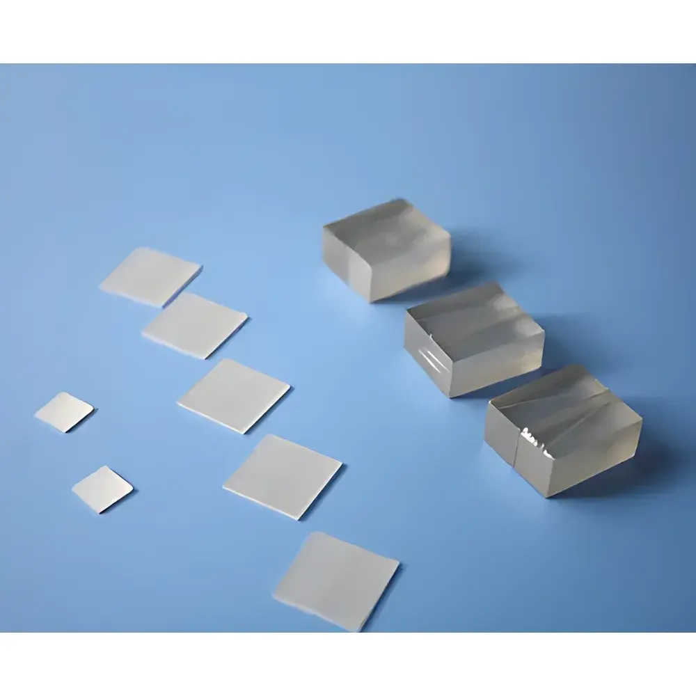
SrTiO3 Bicrystal Substrate Wafers
| Brand | Hefei Kejing |
|---|---|
| Origin | Anhui, China |
| Manufacturer Type | Authorized Distributor |
| Origin Category | Domestic (PRC) |
| Model | Sr-TiO3 |
| Pricing | Available Upon Request |
| Crystal Structure | Cubic |
| Lattice Constant | a = 3.905 Å |
| Growth Method | Flame Fusion (Verneuil) |
| Melting Point | 2080 °C |
| Density | 5.175 g/cm³ |
| Mohs Hardness | 6 |
| Thermal Expansion Coefficient | 9.4 × 10⁻⁶ /°C |
| Dielectric Constant | ~300 (300 K) |
| Loss Tangent | ~5 × 10⁻⁴ (300 K), ~3 × 10⁻⁴ (77 K) |
| Appearance | Transparent (slight brown tint possible depending on annealing history) |
| Chemical Stability | Insoluble in water |
| Orientation Angles | 10°, 24°, 36° (misorientation between two single-crystal domains) |
| Dimensions | 10 × 10 × 0.5 mm, 10 × 5 × 0.5 mm, 5 × 5 × 0.5 mm |
| Surface Finish | Single-side polished, Ra < 0.5 nm |
| Packaging | Class 1000 cleanroom processed |
Overview
SrTiO3 bicrystal substrates are engineered single-crystal wafers consisting of two precisely oriented SrTiO3 domains separated by a well-defined grain boundary—typically fabricated via controlled cleavage and direct bonding or high-precision crystal growth followed by angular lapping and polishing. These substrates serve as foundational platforms for fabricating high-performance grain-boundary Josephson junctions (GBJs), particularly in high-transition-temperature superconducting (HTS) devices such as dc-SQUIDs (Superconducting Quantum Interference Devices). The cubic perovskite structure (space group Pm3m) and lattice parameter of 3.905 Å enable epitaxial integration with common HTS thin films including YBCO (YBa2Cu3O7−δ) and LSCO (La2−xSrxCuO4). Their low dielectric loss (tan δ ≈ 3–5 × 10⁻⁴ across 77–300 K) and thermal expansion compatibility with HTS layers minimize interfacial stress and enhance junction reproducibility—critical for biomagnetic sensing applications including magnetocardiography (MCG) and magnetoencephalography (MEG).
Key Features
- Engineered bicrystal architecture with atomically sharp, low-angle grain boundaries (10°, 24°, and 36° misorientation options)
- Single-side polished surface finish with root-mean-square roughness < 0.5 nm (Ra), verified by atomic force microscopy (AFM)
- High crystalline integrity: twin-free, stoichiometric SrTiO3 confirmed by X-ray diffraction (XRD) rocking curve FWHM < 0.02°
- Thermally stable up to 2080 °C; compatible with standard thin-film deposition processes including pulsed laser deposition (PLD), sputtering, and MBE
- Controlled annealing history ensures consistent optical transmission and minimized oxygen vacancy concentration—essential for reproducible junction critical current density (Jc)
- Class 1000 cleanroom processing and Class 100 clean packaging mitigate particulate contamination during device fabrication
Sample Compatibility & Compliance
These substrates are validated for integration into UHV-compatible thin-film processing workflows and meet baseline material requirements for ISO/IEC 17025-accredited laboratories performing HTS device R&D. While not certified to specific medical device standards (e.g., IEC 60601-2-57), their dimensional stability, surface quality, and dielectric performance align with ASTM F3072–14 (Standard Guide for Characterization of Epitaxial Oxide Thin Films) and support GLP-compliant process documentation when used in regulated research environments. Chemical inertness (insolubility in water, resistance to dilute acids under ambient conditions) ensures compatibility with standard wafer cleaning protocols (e.g., RCA-1/RCA-2, O2 plasma ashing) without substrate degradation.
Software & Data Management
As a passive substrate material, SrTiO3 bicrystals do not incorporate embedded firmware or require proprietary software. However, they are fully compatible with industry-standard metrology platforms—including Keysight B1500A semiconductor parameter analyzers, Lake Shore Cryotronics cryogenic probe stations, and Oxford Instruments Teslatron PT systems—for junction characterization. All lot-specific certification data—including XRD θ–2θ scans, AFM topographs, and optical transmittance spectra—are supplied in ASCII/CSV format and can be imported into MATLAB, Python (NumPy/Pandas), or LabVIEW for statistical process control (SPC) tracking. Traceability includes batch ID, growth date, polishing lot number, and surface inspection report per ANSI/ASQ Z1.4 sampling plans.
Applications
- Grain-boundary Josephson junctions for dc- and rf-SQUID sensors in ultra-low-field biomagnetism
- Heteroepitaxial template for oxide heterostructure studies (e.g., LaAlO3/SrTiO3 interfaces)
- Substrate for resistive switching memristor arrays and ferroelectric tunnel junctions
- Benchmark platform for studying interfacial superconductivity and two-dimensional electron gases (2DEGs)
- Calibration reference for synchrotron-based coherent diffraction imaging (CDI) and ptychography
FAQ
What is the typical grain boundary width in these bicrystal substrates?
Grain boundary widths are sub-nanometer-scale and defined by the misorientation angle; TEM cross-sections confirm coherent interface termination with minimal dislocation density at 10°–24° boundaries.
Are custom off-axis orientations available beyond 10°, 24°, and 36°?
Yes—custom angles from 2° to 45° can be manufactured subject to minimum order quantity and extended lead time (typically 8–12 weeks).
Do you provide XRD rocking curve data for each wafer?
Yes—full θ–2θ and ω-scan data are included in the Certificate of Conformance for every shipped lot.
Is thermal cycling compatibility documented for repeated cool-down/warm-up cycles?
Accelerated thermal cycling tests (77 K ↔ 300 K, 500 cycles) show no measurable change in surface morphology or grain boundary integrity, per post-cycling AFM and SEM inspection.
Can these substrates be used for aqueous electrochemical deposition?
No—they are not recommended for prolonged immersion in aqueous electrolytes due to slow hydrolytic surface degradation above pH 9; use is restricted to dry or vacuum-based thin-film synthesis.

")