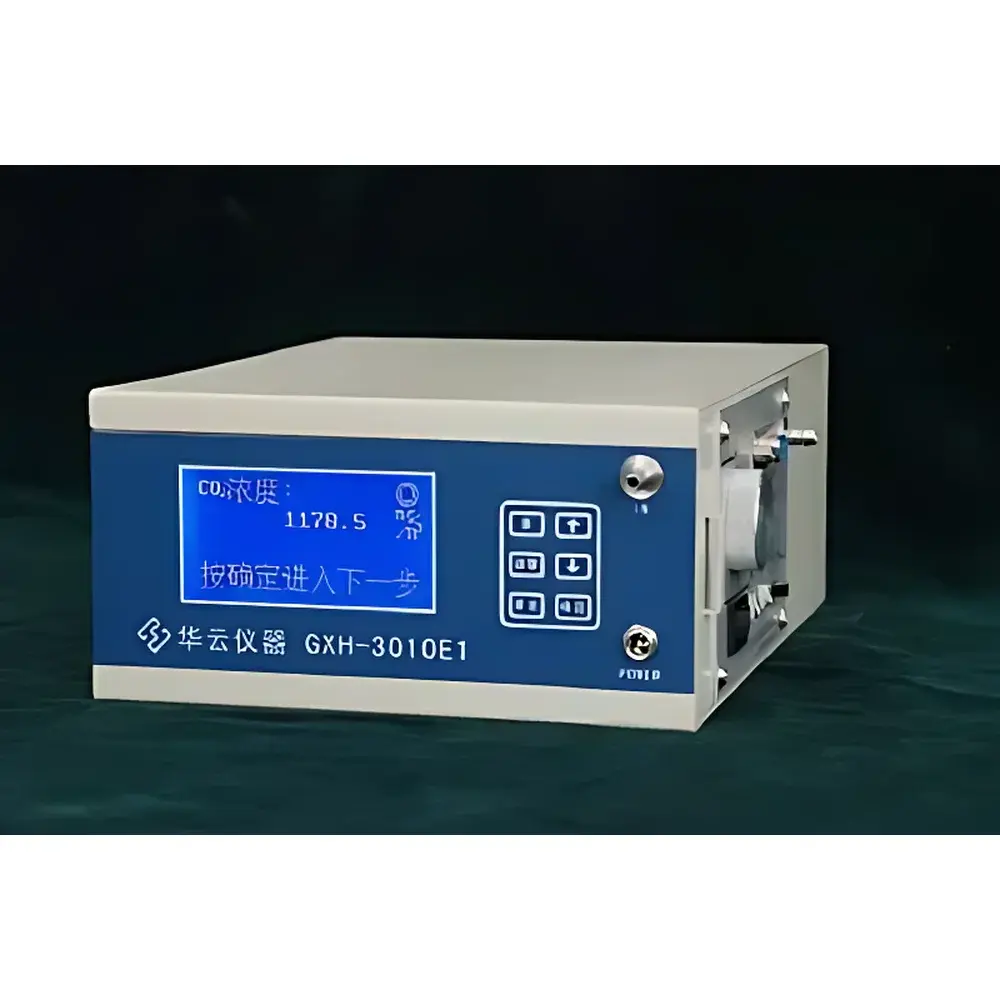
InP Substrate with Semi-Insulating Fe-Doped InGaAs Epitaxial Layer (MOCVD-Grown, Double-Side Polished)
| Brand | 合肥科晶 |
|---|---|
| Origin | USA |
| Manufacturer Type | Authorized Distributor |
| Origin Category | Imported |
| Model | InP-on-InGaAs Semi-Insulating EPI Wafer |
| Price | Upon Request |
| Diameter | 2 inch |
| Crystal Orientation | <100> |
| Substrate Doping | Fe-doped |
| Resistivity | >1×10⁷ Ω·cm |
| EPD | <1×10⁴ cm⁻² |
| Epilayer Type | N-type InGaAs (Si-doped) |
| Lattice Matching | Fully matched to InP |
| Carrier Concentration (Nc) | >2×10¹⁸ cm⁻³ |
| Thickness | 0.5 µm (±20%) |
| Growth Method | MOCVD |
| Surface Finish | Double-side polished |
Overview
This high-purity epitaxial wafer consists of an N-type silicon-doped In0.53Ga0.47As layer lattice-matched to a semi-insulating iron-doped indium phosphide (InP) substrate. Engineered for demanding optoelectronic and high-frequency device fabrication, the structure leverages the near-ideal lattice match (Δa/a 1×10⁷ Ω·cm resistivity) critical for reducing parasitic capacitance and crosstalk in monolithic microwave integrated circuits (MMICs), photodetectors, and heterojunction bipolar transistors (HBTs). Grown via metalorganic chemical vapor deposition (MOCVD) under tightly controlled stoichiometric and thermal conditions, the epilayer exhibits uniform thickness (0.5 µm ±20%), low etch pit density (2×10¹⁸ cm⁻³), enabling reliable process integration in cleanroom environments.
Key Features
- 2-inch diameter -oriented semi-insulating InP substrate with Fe doping for ultra-high bulk resistivity
- Fully lattice-matched N-type InGaAs epilayer (In0.53Ga0.47As) grown by industrial-grade MOCVD
- Silicon doping level optimized for controlled n-type conductivity and thermal stability during device processing
- Double-side chemical-mechanical polishing (CMP) achieving surface roughness <0.2 nm RMS (verified by AFM)
- Low defect density: etch pit density (EPD) <1×10⁴ cm⁻² across full wafer area
- Tight thickness uniformity (±20% across 2″ diameter) validated by spectroscopic ellipsometry and X-ray reflectivity
- Compatible with standard III–V semiconductor processing tools including e-beam lithography, dry etching (BCl₃/Cl₂-based), and dielectric passivation
Sample Compatibility & Compliance
The wafer meets baseline material specifications required for research and pilot-line fabrication under ISO 9001-certified handling protocols. It is suitable for use in Class 100 cleanroom environments and complies with JEDEC JESD22-A108 (high-temperature storage life) and JESD22-A104 (temperature cycling) for pre-fabrication qualification. While not certified to full MIL-STD or space-grade standards, its defect metrics and dopant homogeneity align with typical qualification thresholds for commercial RF and photonic components. Traceability includes batch-specific MOCVD run logs, post-growth XRD rocking curve data, and four-point probe sheet resistance maps — supporting GLP-aligned documentation workflows.
Software & Data Management
No embedded firmware or proprietary software is associated with this passive epitaxial substrate. However, full metrology datasets—including high-resolution XRD θ–2θ scans, SIMS depth profiles (Si dopant distribution), and cross-sectional TEM micrographs—are available upon request for process modeling and TCAD calibration (e.g., Silvaco Atlas, Synopsys Sentaurus). All characterization reports are delivered in vendor-neutral formats (CSV, TIFF, PDF) compliant with FDA 21 CFR Part 11 audit-trail requirements when requested under formal QA agreement.
Applications
- High-electron-mobility transistor (HEMT) channel layers for Ka-band and W-band amplifiers
- Avalanche photodiode (APD) absorption layers operating at 1.3–1.55 µm telecom wavelengths
- Heterostructure infrared detectors (e.g., type-II superlattices on InGaAs buffer stacks)
- Quantum cascade laser (QCL) active region templates requiring low-defect, strain-balanced buffers
- Photonic integrated circuit (PIC) waveguide platforms integrating active InGaAs sections with passive InP cladding
- Calibration reference wafers for Raman spectroscopy and ellipsometric modeling of III–V heterostructures
FAQ
Is this wafer suitable for direct gate-stack deposition without additional surface passivation?
Yes — the double-side polished surface achieves atomic-level termination stability; however, a brief in-situ NH₃ plasma pretreatment is recommended prior to ALD Al₂O₃ or HfO₂ deposition to remove native oxides.
Can the InGaAs layer be selectively etched without undercutting the InP substrate?
Yes — using dilute H₃PO₄:H₂O₂:H₂O (3:1:50) at 25°C, selectivity >25:1 is achievable with minimal InP loss, as confirmed by cross-sectional SEM.
What is the maximum allowable annealing temperature before significant Si dopant diffusion occurs?
Thermal stability testing shows negligible Si redistribution up to 600°C for 30 seconds in N₂; prolonged exposure (>60 s) above 550°C induces measurable tailing in SIMS profiles.
Do you provide wafer mapping data for thickness and carrier concentration?
Yes — full-wafer ellipsometry and Hall-effect mapping (169-point grid) are included in the Certificate of Analysis for each shipment.
Is Fe outdiffusion from the substrate into the InGaAs layer observed during MOCVD growth?
No — secondary ion mass spectrometry (SIMS) confirms Fe concentration remains below detection limit (<5×10¹⁵ cm⁻³) throughout the epilayer, validating effective thermal barrier behavior of the InP/InGaAs interface.
 System")