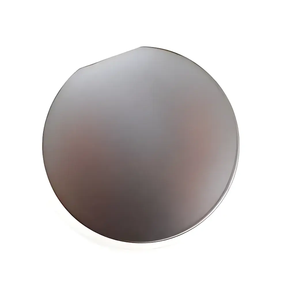
Cu-Coated Silicon Wafer (4″ Dia, 400 nm Polycrystalline Cu on P-Type Si)
| Brand | 合肥科晶 |
|---|---|
| Origin | USA |
| Manufacturer Type | Authorized Distributor |
| Origin Category | Imported |
| Model | Si-on-Cu Thin Film Wafer |
| Price | Upon Request |
| Substrate Diameter | 4 inch (100 mm) or 10×10 mm square |
| Cu Film Thickness | 400 nm |
| Cu Crystallography | Highly Oriented Polycrystalline, Preferential <111> Texture |
| Si Substrate | P-type, Boron-doped, <100> orientation, Single-side polished, Resistivity: 1–20 Ω·cm |
| Surface Roughness | As-grown, Not Specified |
| Packaging | Vacuum-sealed in Class 100 cleanroom bags within Class 1000 cleanroom environment, or individual cassette packaging |
Overview
The Cu-Coated Silicon Wafer (4″ Dia, 400 nm Polycrystalline Cu<111> on P-Type <100> Si) is a precision-engineered substrate designed for advanced thin-film research, microelectronics process development, and materials science characterization. This wafer integrates a highly oriented, 400 nm-thick polycrystalline copper film with strong texture epitaxially deposited onto a single-crystal silicon substrate. The underlying Si substrate is P-type doped with boron, oriented along the crystallographic plane, single-side polished, and exhibits a controlled resistivity range of 1–20 Ω·cm—making it compatible with both semiconductor device prototyping and fundamental interfacial studies. Unlike sputtered or electroplated Cu layers lacking structural control, this film demonstrates high crystallinity and preferred orientation, enabling reproducible investigations into grain boundary diffusion, electromigration behavior, interfacial adhesion, and thermal stability under annealing conditions.
Key Features
- 400 nm thick Cu film with dominant crystallographic texture, confirmed by X-ray diffraction (XRD) and electron backscatter diffraction (EBSD)
- P-type silicon substrate with tight resistivity specification (1–20 Ω·cm) and single-side polish for uniform film nucleation
- As-grown surface roughness—optimized for minimal post-deposition processing while maintaining interface integrity
- Available in standard 4-inch (100 mm) diameter format or custom 10×10 mm square chips for focused beam analysis (e.g., TEM lamella preparation or nanoindentation)
- Manufactured under ISO Class 5 (Class 100) cleanroom conditions and packaged in vacuum-sealed, static-dissipative cleanroom bags compliant with SEMI E10 standards
- No native oxide disruption at the Cu/Si interface—enabling direct integration into UHV-based surface science experiments or in-situ TEM studies
Sample Compatibility & Compliance
This wafer is engineered for compatibility with a broad spectrum of analytical and fabrication platforms, including scanning electron microscopy (SEM), transmission electron microscopy (TEM), X-ray photoelectron spectroscopy (XPS), Auger electron spectroscopy (AES), and atomic force microscopy (AFM). Its defined crystallographic and electrical properties support calibration traceability per ASTM F1529 (Standard Guide for Evaluating Electrical Characteristics of Silicon Wafers) and alignment with ISO/IEC 17025 requirements for reference material qualification. While not certified as a primary reference material, its batch-to-batch consistency—verified via Rutherford backscattering spectrometry (RBS) and four-point probe sheet resistance mapping—supports GLP-compliant experimental workflows in academic, government, and industrial R&D laboratories.
Software & Data Management
As a passive reference substrate, this Cu-coated Si wafer does not incorporate embedded sensors or firmware. However, its metrological specifications are fully documented in accompanying Certificate of Conformance (CoC), which includes lot-specific XRD pole figure data, sheet resistance measurements, and substrate resistivity verification reports. Digital documentation follows NIST-traceable metadata conventions and is compatible with laboratory information management systems (LIMS) supporting ISO/IEC 17025 audit trails. For automated inventory tracking, each wafer shipment includes a serialized barcode label compliant with GS1-128 standards, enabling integration into enterprise resource planning (ERP) systems used in semiconductor pilot-line operations.
Applications
- Model system for studying Cu/Si interfacial reactions during rapid thermal annealing (RTA) and solid-phase epitaxy (SPE)
- Baseline substrate for evaluating barrier layer performance (e.g., TaN, TiN, CoWP) in Cu interconnect integration schemes
- Calibration standard for thickness-sensitive techniques such as ellipsometry, XRF, and SIMS depth profiling
- Platform for investigating stress evolution and hillock formation in sub-micron Cu films under thermal cycling
- Substrate for seed-layer optimization in electrochemical deposition (ECD) process development
- Reference material for validating in-situ synchrotron X-ray scattering during thin-film growth kinetics studies
FAQ
Is the Cu film deposited via sputtering or electrochemical methods?
The Cu film is deposited using ultra-high-vacuum (UHV) magnetron sputtering under controlled Ar partial pressure and substrate temperature, enabling preferential texture development without post-deposition annealing.
Can this wafer be used for high-temperature annealing experiments?
Yes—its thermal budget supports annealing up to 400 °C in inert or forming gas ambient; Cu agglomeration onset is typically observed above 450 °C depending on dwell time and atmosphere.
Are cross-sectional TEM samples available?
Custom cross-section lamellae prepared via focused ion beam (FIB) can be supplied upon request, with orientation alignment verified by pre-FIB EBSD mapping.
What is the typical Cu film resistivity measured at room temperature?
Sheet resistance averages 25–35 mΩ/□ for the 400 nm film, corresponding to a bulk-like resistivity of ~1.8–2.2 µΩ·cm, consistent with highly ordered polycrystalline Cu.
Do you provide batch-specific XRD or SEM micrographs?
Yes—each shipment includes a digital dossier containing grazing-incidence XRD (GIXRD) scans, plan-view SEM images at ×50k magnification, and AFM topography maps (5×5 µm²) acquired in tapping mode.