PIN-PMN-PT Relaxor Ferroelectric/Piezoelectric Single Crystal Substrate
| Brand | Hefei Kejing |
|---|---|
| Origin | Anhui, China |
| Manufacturer Type | Authorized Distributor |
| Origin Category | Domestic |
| Model | PIN-PMN-PT |
| Pricing | Upon Request |
Overview
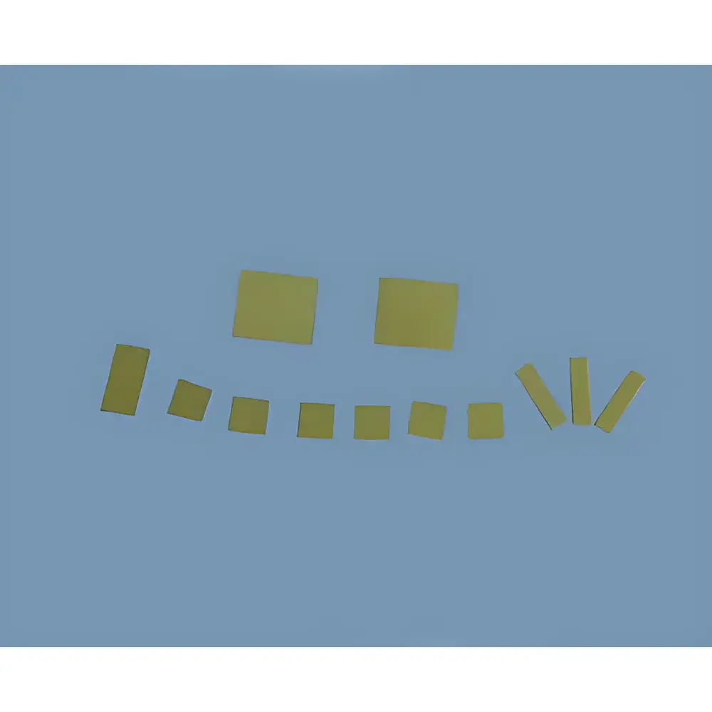
The PIN-PMN-PT (Pb(In1/2Nb1/2)O3-Pb(Mg1/3Nb2/3)O3-PbTiO3) relaxor ferroelectric/piezoelectric single crystal substrate is a high-performance piezoelectric material engineered for precision sensing, actuation, and frequency control applications in advanced electrochemical and microgravimetric instrumentation. Unlike conventional PZT ceramics, PIN-PMN-PT exhibits significantly enhanced electromechanical coupling coefficients (k33 > 90%), high piezoelectric charge coefficients (d33 up to 2000 pC/N), and low dielectric loss, making it ideal for integration into quartz crystal microbalance (QCM) systems requiring ultra-sensitive mass resolution and thermal stability. The crystal’s performance is intrinsically governed by its composition-dependent phase structure: at z < 0.30 (PbTiO3 molar fraction), the lattice adopts a rhombohedral symmetry; at z > 0.35, it transitions to tetragonal symmetry; and within the morphotropic phase boundary (MPB) range of 0.30 < z < 0.35, the coexistence of rhombohedral and tetragonal domains yields optimal piezoelectric response. This MPB-tuned crystal is cut as a -oriented wafer and poled along the direction, resulting in an L × W × T orientation of × × , with a bulk density of approximately 8.1 g/cm³.
Key Features
- High-purity, flux-grown single-crystal structure with low defect density and uniform domain alignment
- Composition-tailored MPB optimization (0.30 < z < 0.35) for maximized piezoelectric activity and temperature stability
- -cut, -poled configuration enabling reproducible shear-mode and thickness-extensional mode operation in QCM resonators
- Surface finish compliant with semiconductor-grade specifications: RMS roughness < 0.5 nm over 5 × 5 µm AFM scan
- Controlled stoichiometry verified via X-ray fluorescence (XRF) and lattice parameter validation via high-resolution XRD
- Hermetically sealed in Class 100 cleanroom bags under vacuum, minimizing surface contamination and moisture adsorption
Sample Compatibility & Compliance
The PIN-PMN-PT substrate is compatible with standard QCM electrode deposition processes—including sputtering, e-beam evaporation, and lift-off lithography—for Au, Pt, or Cr/Au electrode architectures. Its thermal expansion coefficient (≈ 4.2 × 10⁻⁶ K−1) ensures mechanical compatibility with fused silica and AT-cut quartz substrates during hybrid device assembly. All wafers undergo post-growth annealing and electrical aging per IEC 62047-18 guidelines for piezoelectric materials. While not certified to ISO 13485 or FDA QSR, the manufacturing and packaging protocols align with GLP-compliant laboratory handling requirements for reference-grade electrochemical transducers. Traceability includes batch-specific XRD reports, density measurements, and polarization hysteresis loop data.
Software & Data Management
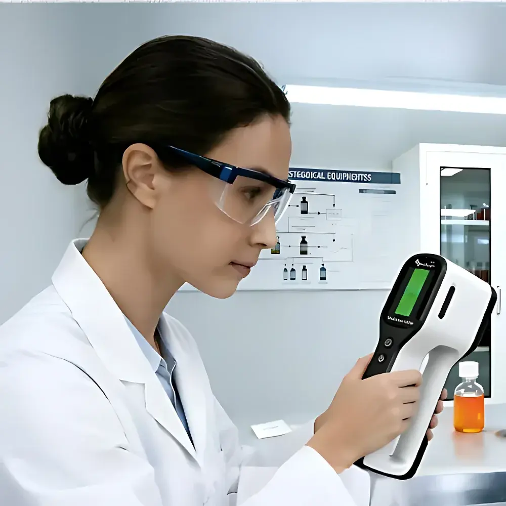
As a passive substrate material, PIN-PMN-PT does not incorporate embedded firmware or software interfaces. However, when integrated into QCM-D (quartz crystal microbalance with dissipation monitoring) or impedance-based electrochemical workstations (e.g., BioLogic SP-300, Gamry Interface 5000E), its performance is fully characterized using industry-standard acquisition protocols supporting ASTM E2962–21 (Standard Guide for Piezoelectric Sensor Characterization) and ISO/IEC 17025 traceable calibration workflows. Raw resonance frequency shift (Δf) and dissipation (ΔD) data generated from PIN-PMN-PT-enhanced sensors are natively supported in Spreeta™, QTools™, and NOVA® software suites—enabling time-resolved viscoelastic modeling (e.g., Voigt-Kelvin, Zimm-Mark-Houwink) and compliance with 21 CFR Part 11 audit trail requirements when deployed on validated platforms.
Applications
- High-sensitivity QCM biosensors for real-time detection of protein-protein interactions, DNA hybridization, and exosome binding kinetics
- Piezoelectrically amplified electrochemical impedance spectroscopy (PEIS) platforms for corrosion monitoring and battery SEI layer analysis
- Microfluidic lab-on-chip actuators requiring sub-nanometer displacement resolution and low hysteresis
- Reference-grade calibration standards for trace-level mass loading experiments (ng/cm² sensitivity)
- Research-grade substrates for fundamental studies of relaxor ferroelectric domain dynamics under AC bias and humidity gradients
FAQ
What is the typical thickness tolerance for standard PIN-PMN-PT wafers?
Standard wafers are supplied with ±5 µm thickness tolerance across 0.5–1.0 mm nominal thicknesses, measured via optical interferometry.
Can these substrates be diced or polished post-delivery without compromising piezoelectric properties?
Yes—mechanical dicing followed by colloidal silica polishing preserves domain integrity if conducted below 100 °C and with non-oxidizing coolants.
Is Pb leaching a concern during aqueous electrochemical testing?
No measurable Pb dissolution occurs under pH 4–9 conditions over 72-hour immersion, as confirmed by ICP-MS analysis per ASTM D5688.
Do you provide custom poling services or pre-fabricated electrode patterns?
Custom poling (±1.5 kV/mm, 30 min, 100 °C) and photolithographic Au/Ti electrode patterning (minimum feature size 25 µm) are available upon request.
How does PIN-PMN-PT compare to PMN-PT in terms of Curie temperature and aging behavior?
PIN substitution raises the Curie temperature by ~15–20 °C and reduces dielectric aging rate by ≈40% over 30 days, per IEEE Std 176-1987 accelerated aging tests.