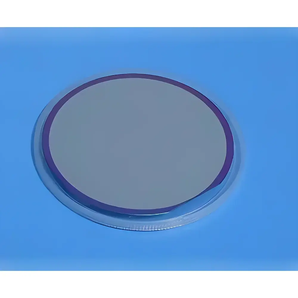
合肥科晶 Si/SiO₂/Ti/Pt(111) Multilayer Thin-Film Substrate on -Oriented Silicon Wafer (2-inch, Imported Grade)
| Brand | Hefei Kejing |
|---|---|
| Origin | USA |
| Distributor Type | Authorized General Distributor |
| Origin Category | Imported |
| Model | Si/SiO₂/Ti/Pt(111) |
| Silicon Substrate | p-type, resistivity 5–10 Ω·cm |
| SiO₂ Thickness | 300 nm |
| Ti Adhesion Layer | 10 nm |
| Pt(111) Top Layer | 150 nm |
| Maximum Thermal Budget | ≤750 °C for 1 h |
| Wafer Diameter | 2 inch (50.8 mm ± 0.5 mm) |
| Thickness | 279 µm |
| Surface Finish | Single-side polished |
| Packaging | Vacuum-sealed in Class 100 cleanroom bags (Class 1000 cleanroom processed) or individual cassette packaging |
Overview
This high-purity multilayer thin-film substrate is engineered for advanced microfabrication, surface science investigations, and epitaxial growth studies requiring well-defined crystalline orientation and controlled interfacial chemistry. The structure consists of a -oriented p-type silicon wafer (5–10 Ω·cm), thermally grown SiO₂ (300 nm), a sputtered titanium adhesion layer (10 nm), and a magnetron-sputtered platinum film with preferential (111) crystallographic texture (150 nm). The Pt(111) orientation is critical for applications demanding low surface energy, high catalytic activity, and lattice-matched heteroepitaxy—such as spintronic device fabrication, electrochemical sensor development, and model catalyst characterization. The substrate’s thermal stability—validated up to 750 °C for one hour—enables compatibility with standard semiconductor processing steps including annealing, metal lift-off, and dielectric deposition without significant interdiffusion or dewetting.
Key Features
- Crystallographically defined architecture: -oriented Si base ensures consistent out-of-plane alignment for subsequent Pt(111) growth via physical vapor deposition.
- Controlled interfacial stack: Thermally grown SiO₂ provides electrical isolation and chemical passivation; ultra-thin Ti (10 nm) ensures robust Pt adhesion while minimizing interfacial resistance.
- Pt(111) texture fidelity: Achieved through optimized sputter parameters and substrate temperature control—confirmed by XRD θ–2θ scans and pole figure analysis.
- Process-compatible geometry: Standard 2-inch diameter (50.8 mm ± 0.5 mm), 279 µm thickness, single-side polished surface meets SEMI specifications for handling in automated cluster tools.
- Ultra-clean delivery: Fabricated and packaged in ISO Class 4 (100-class) cleanroom environments within a broader ISO Class 6 (1000-class) facility; vacuum-sealed in static-dissipative, particle-free bags.
Sample Compatibility & Compliance
The substrate is compatible with standard photolithography, e-beam lithography, reactive ion etching (RIE), and atomic layer deposition (ALD) processes. Its thermal budget allows integration into backend-of-line (BEOL) fabrication flows where post-metallization anneals are required. While not certified to a specific regulatory standard, the manufacturing protocol adheres to ISO 14644-1 Class 4 cleanroom requirements, and documentation supports traceability per ISO 9001 quality management systems. For GLP/GMP-aligned research, full lot-level QC data—including sheet resistance mapping (4-point probe), surface roughness (AFM, RMS < 0.3 nm over 1 × 1 µm), and XRD phase verification—is available upon request.
Software & Data Management
No embedded firmware or proprietary software is associated with this passive substrate. However, it is fully compatible with industry-standard metrology platforms: Keysight B1500A for IV/CV characterization, Bruker D8 Discover for in-situ XRD, and KLA RS-200 for optical reflectometry. All delivered substrates include a certificate of conformance (CoC) listing batch ID, deposition dates, QC test summaries, and storage conditions. Digital records—including raw AFM topographs and XRD patterns—are archived for 5 years and accessible under NDA for audit purposes, supporting FDA 21 CFR Part 11–compliant data integrity workflows when integrated into regulated R&D environments.
Applications
- Model electrode platforms for fundamental electrocatalysis studies (e.g., oxygen reduction, hydrogen evolution).
- Seed layers for epitaxial growth of complex oxides (e.g., PZT, LSMO) in oxide electronics research.
- Reference standards in scanning probe microscopy (SPM) tip calibration and tunneling spectroscopy.
- Test vehicles for evaluating thin-film stress evolution, interdiffusion kinetics, and interfacial reaction barriers under thermal cycling.
- Substrates for fabricating superconducting quantum interference devices (SQUIDs) and magnetic tunnel junctions (MTJs) requiring atomically ordered Pt bottom electrodes.
FAQ
Is the Pt layer polycrystalline or truly (111)-textured?
XRD pole figure analysis confirms strong (111) fiber texture with rocking curve FWHM ≤ 4.5°, indicating dominant out-of-plane alignment and in-plane rotational symmetry.
Can these wafers be cleaved or diced without delamination?
Mechanical dicing using diamond-blade saws with deionized water coolant is validated; plasma dicing (e.g., Bosch process) is not recommended due to potential Pt oxidation and Ti interlayer attack.
What is the typical sheet resistance of the Pt(111) film?
Measured range: 2.1–2.4 Ω/sq at 25 °C (4-point probe, 1 mm spacing), consistent with bulk Pt resistivity and minimal grain boundary scattering.
Are custom thicknesses or alternative adhesion layers (e.g., Cr, NiCr) available?
Yes—custom stacks (e.g., Si/SiO₂/NiCr/Pt or variable Pt thickness from 50–300 nm) are offered under non-standard order (NSO) terms with minimum batch size of 5 wafers.
Does the SiO₂ layer withstand HF-based wet etches?
The 300 nm thermal oxide exhibits standard etch rate of ~0.8 nm/s in 1% HF at 25 °C; BOE (6:1) reduces rate to ~0.3 nm/s—suitable for selective lift-off schemes with appropriate masking.