Ge Crystal Substrates (合肥科晶 | Ge Single-Crystal Wafers for QCM and Semiconductor Applications)
| Brand | Hefei Kejing |
|---|---|
| Origin | Anhui, China |
| Manufacturer Type | Authorized Distributor |
| Origin Category | Domestic |
| Model | Ge |
| Pricing | Upon Request |
| Crystal Structure | Cubic, a = 5.6754 Å |
| Growth Method | Czochralski (CZ) |
| Density | 5.765 g/cm³ |
| Melting Point | 937.4 °C |
| Thermal Conductivity | 64 W/(m·K) |
| Doping Types | Undoped / Sb-doped (n-type) / Ga-doped (p-type) |
| Resistivity Range | >35 Ω·cm (undoped), 0.05 Ω·cm (Sb), 0.05–0.1 Ω·cm (Ga) |
| Etch Pit Density (EPD) | < 4 × 10³ cm⁻² |
| Orientations Available | <100>, <110>, <111> ± 0.5° |
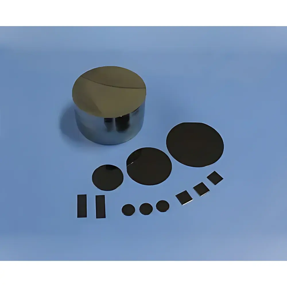
| Standard Dimensions | Ø25.4 mm × 0.5 mm, Ø50.8 mm × 0.5 mm, Ø101.6 mm × 0.5 mm |
| Surface Finish | As-cut or mechanically polished (<110>: Ra < 5 Å, non-chemical polish) |
| Packaging | Class 1000 cleanroom + Class 100 clean bag or individual wafer cassette |
Overview
Ge crystal substrates are high-purity single-crystal germanium wafers engineered for precision applications in quartz crystal microbalance (QCM) sensor development, infrared (IR) optical component fabrication, semiconductor device prototyping, and photovoltaic research. Germanium’s narrow bandgap (0.67 eV at 300 K), high refractive index (~4.0 in mid-IR), and excellent carrier mobility make it uniquely suited for IR-transparent windows, ATR prisms, heteroepitaxial templates, and mass-sensitive transducer platforms. These substrates are grown via the Czochralski method under controlled inert atmosphere, ensuring low dislocation density (EPD < 4 × 10³ cm⁻²) and lattice uniformity essential for reproducible thin-film deposition and surface acoustic wave (SAW) device integration. Unlike silicon or sapphire, Ge offers superior transmission from 2–14 µm—enabling direct use in Fourier-transform infrared (FTIR) spectroscopy cells and gas-sensing QCM configurations where substrate absorption must be minimized.
Key Features
- Single-crystal germanium wafers with certified orientation tolerances of ±0.5° for , , and planes—critical for epitaxial alignment and anisotropic etching processes
- Controlled doping options: undoped (high-resistivity >35 Ω·cm), antimony-doped (n-type, ~0.05 Ω·cm), and gallium-doped (p-type, 0.05–0.1 Ω·cm) to support varied charge transport requirements
- Surface roughness <5 Å RMS on -oriented wafers in as-cut condition—eliminates need for aggressive chemical-mechanical polishing while maintaining atomic-level flatness for molecular adsorption studies
- Thermal conductivity of 64 W/(m·K) enables stable temperature management during in situ QCM measurements under variable thermal loads
- Supplied in ISO Class 1000 cleanroom environments and packaged in Class 100 clean bags or rigid single-wafer cassettes to prevent particulate contamination and oxide formation
- Customizable geometry: diameter (Ø25.4 mm to Ø101.6 mm), thickness (standard 0.5 mm, adjustable per specification), and off-axis angle upon request
Sample Compatibility & Compliance
These Ge substrates are compatible with standard vacuum-based thin-film deposition systems (e-beam evaporation, sputtering, MBE), wet chemical processing (HCl:H₂O₂:H₂O, NH₄OH:H₂O₂:H₂O), and plasma-enhanced surface functionalization. They meet ASTM F1529-21 specifications for semiconductor-grade germanium wafer dimensional tolerances and surface quality. For regulated laboratory environments—including GLP-compliant analytical development labs—the substrates are traceable to material certificates listing batch-specific EPD, resistivity, and orientation verification data. While Ge itself is not subject to RoHS exemption clauses, all handling and packaging materials comply with IEC 61249-2-21 for halogen-free cleanroom consumables.
Software & Data Management
Though passive substrates do not embed firmware or onboard electronics, their metrological traceability integrates seamlessly into instrument control ecosystems. When used in QCM-D (quartz crystal microbalance with dissipation monitoring) or impedance-based sensing platforms, Ge wafers serve as calibrated mechanical reference surfaces—enabling baseline drift correction and frequency shift normalization across multi-cycle adsorption/desorption experiments. Raw crystallographic data (XRD pole figures, rocking curve FWHM) and surface topography (AFM line scans) are provided in vendor-supplied QC reports, formatted for import into MATLAB, Python (NumPy/Pandas), or LabArchives ELN systems. All documentation adheres to ALCOA+ principles (Attributable, Legible, Contemporaneous, Original, Accurate, Complete, Consistent, Enduring, Available) to support FDA 21 CFR Part 11 audit readiness.
Applications
- Infrared optical components: Fabrication of anti-reflection coated windows, beam splitters, and internal reflection elements for FTIR and tunable diode laser absorption spectroscopy (TDLAS)
- QCM sensor development: High-mass-sensitivity platforms for real-time detection of volatile organic compounds (VOCs), heavy metal ions, and biomolecular binding events in liquid phase
- Heteroepitaxial growth: Template layers for III–V compound semiconductors (e.g., GaAs on Ge) in multi-junction solar cells and integrated photonics
- Calibration standards: Reference substrates for Raman spectroscopy intensity normalization and ellipsometry modeling of thin-film dielectric functions
- Surface science studies: UHV-compatible platforms for XPS, AES, and LEED analysis of adsorbate-induced surface reconstruction
FAQ
Are these Ge substrates suitable for high-vacuum or ultra-high-vacuum (UHV) applications?
Yes—low outgassing rates and absence of binder residues make them compatible with base pressures down to 1 × 10⁻¹⁰ mbar when pre-baked at 200 °C for 2 hours.
Can I specify custom crystallographic orientations beyond , , and ?
Yes—off-axis orientations (e.g., 4° miscut) are available; lead time increases by 10–14 business days for XRD verification.
Do you provide surface characterization data (AFM, XRD, XPS) with each shipment?
Standard shipments include EPD, orientation, and resistivity certification. Full surface metrology reports (AFM roughness, XRD rocking curves) are available upon request at no additional cost.
What is the maximum operating temperature for Ge substrates in continuous use?
For structural integrity under thermal cycling, sustained operation is recommended below 600 °C; short-term exposure up to 800 °C is permissible with controlled ramp rates ≤5 °C/min.
Is hydrogen annealing supported for native oxide removal prior to deposition?
Yes—annealing in 5% H₂/Ar at 400–450 °C for 15 minutes effectively removes GeO₂ without inducing surface roughening or step bunching.
Related Products