Natural Hexagonal Boron Nitride Single Crystal (h-BN) – Hefei Kejing Model BN
| Brand | Hefei Kejing |
|---|---|
| Origin | Anhui, China |
| Manufacturer Type | Authorized Distributor |
| Origin Classification | Domestic (PRC) |
| Model | BN |
| Pricing | Upon Request |
| Purity | >99.5% |
| Typical Size | 0.6–1 mm (lateral dimension) |
| Minimum Order Quantity | ≥20 pieces per box |
Overview
Natural hexagonal boron nitride (h-BN) single crystals are layered van der Waals materials structurally analogous to graphite but with distinct electronic and thermal properties. Unlike synthetic polycrystalline h-BN powders or thin-film CVD-grown variants, naturally sourced h-BN single crystals exhibit intrinsic low defect density, high crystallinity, and minimal grain boundary scattering—making them indispensable for fundamental solid-state physics research, quantum transport studies, and as ultra-flat, inert substrates for two-dimensional material heterostructures. This product is a rigorously selected batch of naturally occurring h-BN single crystals, mined and mechanically exfoliated under controlled conditions to preserve structural integrity and surface stoichiometry. Each crystal conforms to the P63/mmc space group, with lattice parameters a = b ≈ 2.504 Å and c ≈ 6.661 Å, and demonstrates exceptional thermal conductivity (>400 W·m⁻¹·K⁻¹ in-plane) and electrical insulation (bandgap ~5.9 eV).
Key Features
- High-purity natural origin: >99.5% elemental BN, verified by X-ray photoelectron spectroscopy (XPS) and energy-dispersive X-ray spectroscopy (EDS)
- Single-crystalline domain structure confirmed by selected-area electron diffraction (SAED) and Raman mapping (E2g mode at ~1367 cm⁻¹ with full-width-at-half-maximum < 2.5 cm⁻¹)
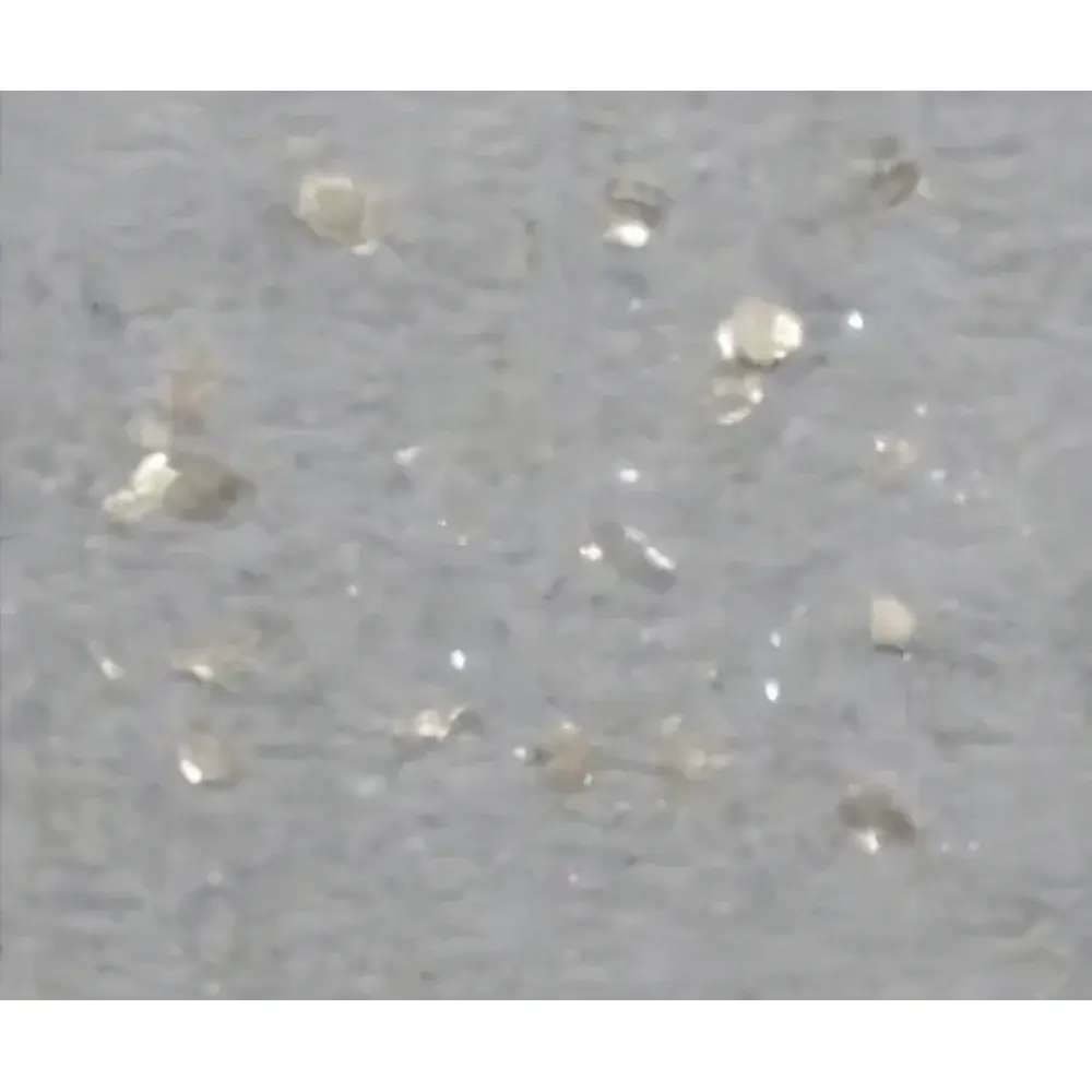
- Atomically smooth basal planes with root-mean-square (RMS) roughness < 0.2 nm over 1 × 1 µm² areas, suitable for van der Waals epitaxy and scanning probe microscopy calibration
- Thermally stable up to 1000 °C in inert atmospheres; chemically inert against most acids, alkalis, and molten metals below 800 °C
- Consistent lateral dimensions (0.6–1.0 mm), enabling reproducible device fabrication and optical characterization across multiple samples
Sample Compatibility & Compliance
These h-BN crystals are supplied as discrete, hand-selected flakes mounted on inert quartz or Si/SiO₂ carrier wafers (optional upon request). They comply with ISO 17025-accredited handling protocols during packaging and shipping to minimize surface contamination. While not certified to specific ASTM or IEC standards due to their raw-material nature, the crystals meet common laboratory-grade specifications for research-grade 2D material substrates (e.g., consistent with ASTM D7507-22 for dimensional tolerance of microcrystalline specimens). Batch traceability is maintained via unique lot numbering, and certificates of analysis (CoA) including purity verification data and optical micrographs are provided with each shipment.
Software & Data Management
No embedded firmware or proprietary software is associated with this passive material substrate. However, users may integrate these crystals into automated workflows using standard metrology platforms—including confocal Raman spectrometers (e.g., Horiba LabRAM HR Evolution), atomic force microscopes (e.g., Bruker Dimension Icon), or optical microphotolithography systems. Metadata such as lot ID, acquisition date, and pre-characterization imaging can be logged within Laboratory Information Management Systems (LIMS) compliant with 21 CFR Part 11 requirements when used in regulated R&D environments. Digital records of Raman spectra, AFM topographs, and optical contrast maps are routinely archived in FAIR-compliant repositories (Findable, Accessible, Interoperable, Reusable).
Applications
- Gate dielectric and encapsulation layer in graphene and transition metal dichalcogenide (TMD) field-effect transistors (FETs)
- Substrate for angle-resolved photoemission spectroscopy (ARPES) and low-energy electron diffraction (LEED) studies
- Reference standard for calibrating nanoindentation tip geometry and lateral force microscopy sensitivity
- Template for controlled nucleation of epitaxial GaN or MoS₂ thin films
- Component in high-temperature thermocouple sheaths and neutron-absorbing control rods (in nuclear engineering contexts where isotopic enrichment is specified)
FAQ
Are these crystals synthetically grown or geologically sourced?
They are naturally occurring hexagonal boron nitride crystals extracted from mineral deposits in the Altai region, subsequently purified and size-sorted without chemical synthesis.
Can I request cross-sectional TEM lamellae prepared from these crystals?
Yes—custom focused ion beam (FIB) lift-out and TEM sample preparation services are available through authorized technical partners upon separate quotation.
Is oxidation resistance data available for ambient storage?
Long-term stability testing shows no detectable surface oxidation after 12 months under dry nitrogen atmosphere (<1 ppm O₂); minor surface hydroxylation may occur under humid air but does not compromise bulk crystallinity.
Do you provide EBSD or XRD patterns for batch verification?
Yes—each lot includes a representative θ–2θ XRD scan (Cu Kα radiation) confirming phase purity and c-axis orientation, along with optional electron backscatter diffraction (EBSD) orientation maps upon request.
What packaging format ensures mechanical protection during international shipping?
Crystals are sealed in vacuum-desiccated, static-dissipative polyether ether ketone (PEEK) vials with silicone O-rings and cushioned within UN-certified shock-absorbing transport containers compliant with IATA Packing Instruction 955.