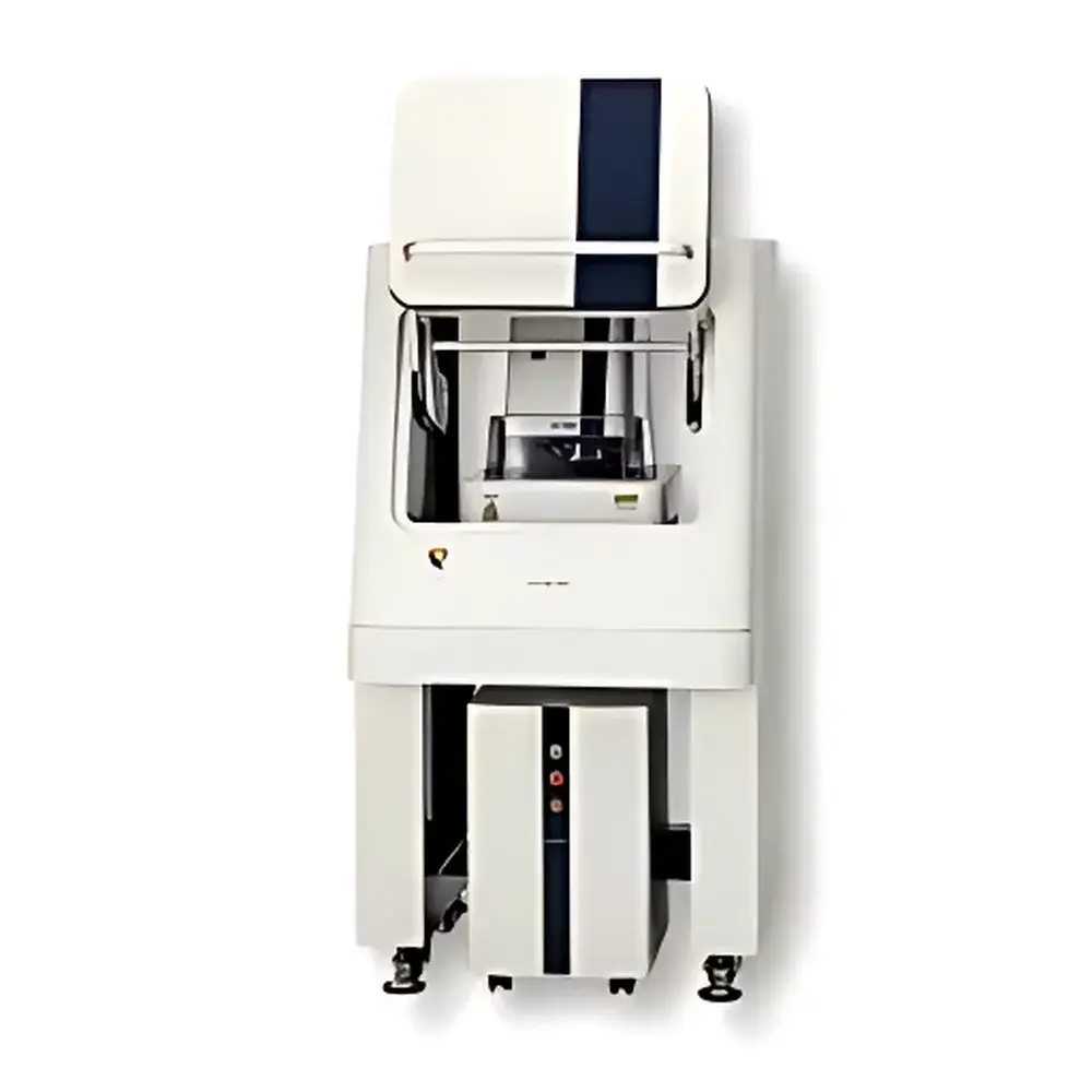
Hitachi AFM5500M II Fully Automated Scanning Probe Microscope
| Brand | Hitachi |
|---|---|
| Origin | Japan |
| Manufacturer Type | Original Equipment Manufacturer (OEM) |
| Product Category | Imported Instrument |
| Model | AFM5500M II |
| Instrument Type | Atomic Force Microscope (AFM) |
| Application Class | Materials Science AFM |
| Position Detection Noise | ≤ 0.04 nm (High-Resolution Mode) |
| Sample Diameter | ≤ 100 mm |
| Sample Thickness | ≤ 20 mm |
| XY Stage Travel Range | 100 mm × 100 mm |
Overview
The Hitachi AFM5500M II is a fully automated, high-precision atomic force microscope engineered for advanced materials characterization in research and industrial quality control laboratories. Built upon Hitachi High-Technologies’ proprietary scanning probe platform, it employs a closed-loop, piezoelectric tube-free XY scanner architecture—eliminating inherent arc-motion distortion common in conventional tube scanners—and integrates a crosstalk-free Z-scanner to ensure sub-nanometer vertical fidelity without horizontal image warping. Unlike open-loop systems, the AFM5500M II’s hardware-level coordinate stability enables true quantitative topography, mechanical property mapping, and electrostatic potential analysis with traceable metrological integrity. Its design conforms to the functional requirements of ISO/IEC 17025-accredited labs and supports audit-ready workflows aligned with GLP and GMP principles.
Key Features
- Fully Automated Operation: Integrated robotic probe handling, auto-alignment of optical lever path, real-time parameter optimization, and one-click acquisition–processing–analysis sequencing reduce operator dependency and enhance inter-user reproducibility.
- Distortion-Free Scanning Architecture: A newly developed planar XY scanner replaces traditional tube-based designs, removing curvature-induced geometric artifacts and enabling accurate flat-surface reconstruction without reliance on post-hoc software correction.
- Crosstalk-Free Vertical Actuation: The Z-scanner is mechanically decoupled from lateral motion, preventing bending-induced horizontal displacement during vertical extension—critical for accurate slope measurement on crystalline surfaces such as photovoltaic absorber layers.
- SIS (Sampling Intelligent Scan) Mode: Dynamically positions the probe only at designated sampling points, minimizing lateral shear forces and tip wear while preserving fragile or high-adhesion samples—including amorphous silicon thin films and nanostructured electrodes.
- Multi-Modal Property Mapping: Simultaneous acquisition of topography, elastic modulus (via SIS-QuantiMech), deformation, adhesion, friction, conductivity, piezoelectric response, and surface potential—enabling correlative structure–property analysis.
- Dual-Mode Kelvin Probe Force Microscopy (KFM): Supports both amplitude-modulation KFM (AM-KFM) for comparative work-function analysis across homogeneous phases and frequency-modulation KFM (FM-KFM) for quantitative, high-sensitivity surface potential mapping of heterogeneous composites, e.g., phase-separated organic photovoltaics or ferroelectric domain arrays.
Sample Compatibility & Compliance
The AFM5500M II accommodates wafers and substrates up to 100 mm in diameter and 20 mm in thickness—compatible with standard semiconductor, MEMS, and battery electrode sample formats. Its rigid stage design and vacuum-compatible optional enclosure meet ASTM E2531-21 guidelines for nanoscale dimensional metrology. All measurement modes comply with ISO 25178-601 (areal surface texture) and ISO/TS 19001-2 (nanomechanical property mapping). Data provenance—including instrument configuration, environmental logs, and calibration history—is preserved per FDA 21 CFR Part 11 requirements when used with validated software modules.
Software & Data Management
Control and analysis are performed via Hitachi’s proprietary SPM Station software, which provides full scriptability (Python API), batch processing pipelines, and built-in statistical reporting tools compliant with ISO 5725-2 precision evaluation standards. Raw data is stored in vendor-neutral HDF5 format with embedded metadata (timestamp, operator ID, environmental conditions, feedback gains). Audit trails record all parameter changes, file exports, and user actions—supporting laboratory accreditation under ISO/IEC 17025 Clause 7.7. Optional integration with LIMS platforms enables traceable sample lifecycle management from preparation to final report generation.
Applications
- Quantitative roughness and step-height metrology of SiN, SiO₂, and metal gate stacks in advanced logic nodes
- Mechanical property heterogeneity mapping in polymer-blend dielectrics and solid-state electrolytes
- Surface potential distribution analysis of perovskite solar cell interfaces and grain boundaries
- Correlative AFM–SEM–CSI registration for multi-modal failure analysis of microelectronic packages
- In-process monitoring of thin-film deposition uniformity and defect evolution in roll-to-roll manufacturing
- Dynamic nanomechanical testing under controlled humidity or temperature (with optional environmental chamber)
FAQ
What distinguishes the AFM5500M II’s XY scanner from conventional tube scanners?
It uses a planar, closed-loop piezoelectric actuator system that eliminates arc-motion distortion—ensuring geometric fidelity without post-processing correction.
Can the AFM5500M II perform quantitative elasticity mapping on soft biological samples?
Yes—when operated in SIS-QuantiMech mode with calibrated cantilevers and appropriate force setpoints, it delivers Young’s modulus values traceable to NIST-traceable reference standards.
Is FM-KFM compatible with ambient and liquid environments?
FM-KFM is optimized for ultra-high-resolution work in vacuum and dry nitrogen; AM-KFM remains the preferred mode for ambient or liquid-phase surface potential measurements.
How does the shared-coordinate stage interface with SEM or CSI systems?
Through Hitachi’s proprietary coordinate registration protocol and AFM marker functionality, enabling sub-micron positional repeatability across modalities without manual re-alignment.
Does the system support automated tip qualification and lifetime tracking?
Yes—the integrated probe evaluation module quantifies tip radius degradation in real time using reference gratings and updates tip geometry parameters in analysis scripts accordingly.


