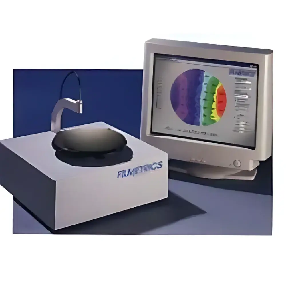
Filmetrics F50/F40 Thin-Film Thickness Measurement System
| Brand | Filmetrics |
|---|---|
| Origin | USA |
| Model(s) | F50, F40 |
| Optical Measurement Principle | Spectral Reflectance Analysis (Visible–NIR) |
| Supported Substrates | Si, glass, Al, GaAs, stainless steel, polycarbonate, polymer films |
| Film Types | Transparent, semi-transparent, absorbing thin films (e.g., SiO₂, SiNₓ, DLC, photoresist, a-Si, poly-Si) |
| Interface | USB 2.0 |
| Software Platform | Filmetrics F20 Suite (Windows-compatible) |
| Preloaded Material Library | >100 optical constants (n, k) |
| Multilayer Capability | Yes, up to 10 layers (with user-defined or fitted optical models) |
| Minimum Measurable Thickness | ~1 nm (dependent on material dispersion and substrate reflectivity) |
| Maximum Measurable Thickness | ~50 µm (for low-absorption dielectrics on reflective substrates) |
| Measurement Speed | <2 seconds per spot |
| Calibration | Factory-calibrated |
Overview
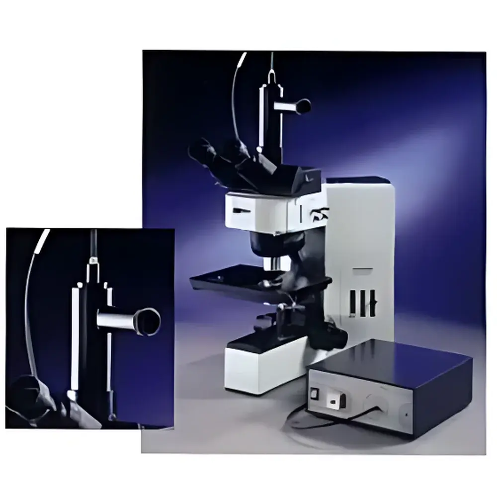
The Filmetrics F50 and F40 are benchtop spectral reflectometry systems engineered for non-contact, non-destructive measurement of thin-film thickness and complex refractive index (n, k) on semiconductor wafers and optoelectronic substrates. Operating on the physical principle of spectral interference analysis, these instruments acquire broadband reflectance spectra (typically 380–1050 nm) from a focused spot (diameter ≈ 20–50 µm), then apply rigorous thin-film optical modeling—based on the Fresnel equations and matrix transfer formalism—to extract layer thicknesses and wavelength-dependent optical constants. Unlike ellipsometers, which require precise angular alignment and polarization control, Filmetrics systems leverage normal-incidence reflectance with high signal-to-noise ratio detectors and factory-optimized spectral response, enabling rapid deployment in fab environments, QC labs, and R&D cleanrooms without dedicated optical alignment expertise.
Key Features
- High-speed acquisition: Full-spectrum capture and model-based fitting completed in under two seconds per measurement location.
- Preloaded optical database: Includes >100 validated n/k datasets for common semiconductor and dielectric materials—including SiO₂, SiNₓ, amorphous silicon, photoresists (e.g., AZ, Shipley), DLC, ITO, and metal oxides—enabling immediate multilayer analysis without prior characterization.
- User-expandable optical library: New materials can be added via optical constant fitting routines using measured spectra from reference samples, supporting proprietary process development and novel stack qualification.
- Robust hardware architecture: Thermally stabilized halogen-tungsten light source, high-resolution CCD spectrometer, and precision fiber-optic probe ensure long-term repeatability (<0.1% RSD for repeated SiO₂-on-Si measurements).
- Wafer-scale compatibility: Integrated XYZ stage option (F50 only) supports automated mapping across 200 mm and 300 mm wafers; manual stage version (F40) is optimized for discrete sample inspection.
- FDA 21 CFR Part 11–ready software: Audit trail logging, electronic signatures, and user-access controls available via optional compliance module for GMP/GLP-regulated environments.
Sample Compatibility & Compliance
The F50/F40 systems are validated for use with planar, rigid substrates exhibiting specular reflectivity ≥15% in the operational spectral range. Compatible base materials include single-crystal silicon (polished or thermally oxidized), fused silica, BK7 glass, aluminum-coated mirrors, GaAs wafers, stainless steel, and engineered polymers (e.g., polycarbonate, PET). Films must be continuous, homogeneous at the measurement spot scale, and exhibit sufficient optical contrast relative to the substrate. Applications span native oxide growth monitoring, PECVD/Sputter-deposited dielectric stacks, lithographic resist spin-coating uniformity, and post-etch film residue assessment. The system complies with ISO/IEC 17025 traceability guidelines for optical metrology and supports documentation workflows aligned with SEMI E10 (Specification of Definition and Measurement of Equipment Reliability, Maintainability, and Availability) and ASTM F398 (Standard Practice for Measuring Thickness of Transparent Films Using Spectral Reflectance).
Software & Data Management
Controlled via the Filmetrics F20 Suite (v6.x or later), the software provides real-time spectral visualization, interactive layer-model construction (including graded interfaces and roughness layers), and batch processing for wafer maps or lot-level statistics. All raw spectra, fitted parameters, and metadata (timestamp, operator ID, instrument serial number, environmental conditions) are stored in encrypted SQLite databases. Export options include CSV, XML, and industry-standard SDF (Semiconductor Data Format) for integration with MES and SPICE modeling tools. For regulated environments, the optional Compliance Pack enables full 21 CFR Part 11 compliance—including immutable audit trails, role-based permissions, and electronic signature enforcement—with validation documentation supplied upon request.
Applications
- Real-time monitoring of thermal oxide growth on Si wafers (0.5–200 nm range).
- Thickness and stoichiometry verification of plasma-enhanced CVD SiNₓ films (refractive index correlates with N/Si ratio).
- Photoresist thickness mapping pre- and post-bake to quantify solvent loss and thermal flow.
- Characterization of transparent conductive oxides (TCOs) such as ITO and AZO for display and PV applications.
- Quality assurance of hard carbon coatings (DLC) on MEMS devices and microfluidic substrates.
- Failure analysis of delamination or interfacial oxidation in bonded wafer stacks.
FAQ
Can the F50/F40 measure films on transparent substrates like bare glass?
Yes—provided the backside is coated with a reflective layer (e.g., aluminum or silver sputter coating) or the sample is placed on a reflective carrier. Uncoated transparent substrates yield ambiguous interference fringes due to multiple reflections.
Is calibration required between measurements?
No. Instruments are factory calibrated using NIST-traceable standards. A daily reference check using a certified SiO₂-on-Si standard wafer is recommended for critical applications but not mandatory for routine use.
What is the minimum resolvable thickness difference across a wafer?
With automated stage mapping (F50), spatial resolution is defined by step size (default 1 mm); thickness repeatability is ±0.1 nm for SiO₂ on Si under controlled lab conditions.
Does the software support custom scripting or API integration?
Yes—the F20 Suite includes a documented COM interface for Python, MATLAB, and LabVIEW, enabling automated measurement sequences and integration into custom fabrication data pipelines.


