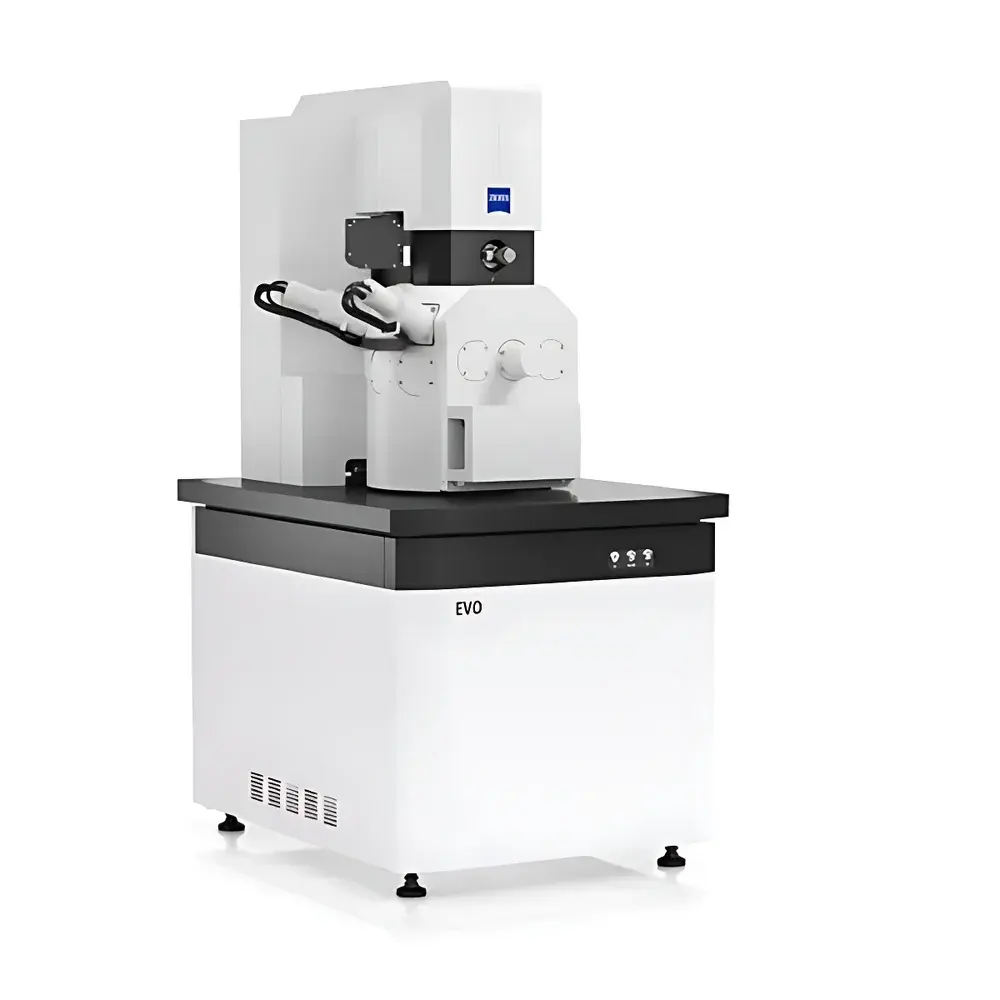
ZEISS EVO Scanning Electron Microscope
| Brand | ZEISS |
|---|---|
| Origin | Shanghai, China |
| Manufacturer Type | Manufacturer |
| Regional Classification | Domestic |
| Model | EVO |
| Quotation | Upon Request |
| Instrument Form Factor | Floor-standing / Conventional Large-scale |
| Electron Source Type | Tungsten Filament |
| SEM Category | Entry-level Tungsten-Filament SEM |
Overview
The ZEISS EVO Scanning Electron Microscope is a robust, floor-standing SEM engineered for routine industrial and academic applications requiring high reproducibility, intuitive operation, and scalable performance. Based on conventional thermionic emission technology using a tungsten (W) or optional lanthanum hexaboride (LaB₆) electron source, the EVO platform delivers stable beam current and consistent imaging across a wide range of accelerating voltages (0.2–30 kV). Its design prioritizes operational flexibility over ultra-high resolution—making it ideal for quality assurance labs, failure analysis teams, and materials characterization departments where throughput, ease of use, and compliance-ready documentation are critical. Unlike field-emission SEMs, the EVO’s tungsten-filament architecture offers lower acquisition and maintenance costs while retaining sufficient resolution (≤3.0 nm at 30 kV, SE mode) and depth of field for structural evaluation of metals, ceramics, polymers, and composites.
Key Features
- Floor-standing mechanical architecture with modular vacuum chamber options: standard, large, and extra-large volumes—enabling accommodation of bulky or irregularly shaped industrial samples up to 200 mm in diameter.
- Three operational vacuum modes: high vacuum (HV), variable pressure (VP), and environmental scanning (ESEM-compatible)—supporting direct imaging of non-conductive, hydrated, or outgassing specimens without metal coating.
- Multi-detector compatibility: Secondary Electron (SE), Backscattered Electron (BSE), Energy-Dispersive X-ray Spectroscopy (EDS/EDX), VP detectors, and Charge Compensation (C2D) for charge mitigation on insulating surfaces.
- Automated workflow integration: motorized stage control, auto-focus, auto-stigmation, and beam alignment routines reduce operator dependency and support GLP-compliant documentation protocols.
- User-configurable system architecture: users select optimal combinations of electron source (W or LaB₆), detector suite, chamber size, and vacuum mode to align technical capability with budgetary and application-specific requirements.
Sample Compatibility & Compliance
The EVO accommodates diverse sample geometries—including cross-sectioned metallurgical mounts, electronic assemblies, coated substrates, and particulate filters—without mandatory conductive sputtering in VP/ESEM mode. Its compatibility with ISO 16232 (road vehicle fluid cleanliness) and VDA 19 Part 1 & 2 (automotive component cleanliness testing) is reinforced by standardized particle detection algorithms, calibrated area measurement tools, and traceable stage positioning. For regulated environments, the system supports audit-trail generation and user-access logging compatible with FDA 21 CFR Part 11 principles when integrated with ZEISS SMART software and validated IT infrastructure. Non-metallic inclusion analysis in steel follows ASTM E45 and ISO 4967 methodologies via BSE contrast imaging and automated phase segmentation.
Software & Data Management
ZEISS SMART software provides a unified interface for acquisition, annotation, measurement, and reporting. It includes built-in templates for ISO/VDA-compliant particle reports, customizable measurement protocols (e.g., Feret diameter, aspect ratio, circularity), and batch processing for multi-image datasets. All image metadata—including kV, working distance, dwell time, detector type, and vacuum mode—is embedded in TIFF and BMP exports. Raw data files adhere to open-format standards (e.g., TIFF with XML metadata headers), enabling third-party analysis in ImageJ/Fiji or MATLAB. Optional ZEISS ZEN Connect enables secure remote instrument monitoring, collaborative annotation, and LIMS integration via RESTful API.
Applications
- Quality Control & Failure Analysis: Imaging of solder joint integrity, wire bond fractures, delamination in PCB laminates, and corrosion morphology on galvanized low-carbon steel (as demonstrated in Zn/Fe interfacial analysis).
- Cleanliness Testing: Automated particle counting and classification on engine components per ISO 16232-C, including morphological filtering (e.g., distinguishing fiber vs. metallic debris) and elemental verification via EDS mapping.
- Materials Science: Phase contrast imaging of multiphase alloys, oxide layer thickness assessment, and grain boundary delineation in heat-treated steels using BSE and topographic SE contrast.
- Electronics Inspection: Low-kV (<5 kV) surface inspection of IC packages and MEMS devices to minimize charging artifacts and preserve fine lithographic features.
- Fuel Cell R&D: Cross-sectional imaging of PEM membranes and Pt/C catalyst layers under 3 kV LaB₆ illumination to resolve nanoscale porosity and interfacial adhesion defects.
FAQ
What electron sources are supported on the ZEISS EVO platform?
The standard configuration uses a tungsten hairpin filament; an optional LaB₆ cathode is available for improved brightness and signal-to-noise ratio at low accelerating voltages (≤5 kV).
Can the EVO perform elemental analysis?
Yes—when equipped with an EDS detector and compatible spectrometer, the system supports qualitative and semi-quantitative elemental mapping and point analysis per ISO 14705 and ASTM E1508.
Is the EVO suitable for uncoated polymer or biological samples?
In Variable Pressure (VP) or Environmental SEM (ESEM) mode, the EVO enables direct imaging of non-conductive specimens without sputter coating, leveraging gas ionization for charge dissipation.
How does the EVO ensure compliance with automotive cleanliness standards?
Through certified particle detection algorithms, calibrated stage movement, and traceable image metadata, the system meets documentation requirements for ISO 16232 and VDA 19 audits when operated within validated SOPs.
What vacuum modes are available, and how do they affect imaging?
High Vacuum (HV) delivers maximum resolution for conductive samples; Variable Pressure (VP) allows imaging of insulators at pressures up to 400 Pa; Environmental mode (with water vapor or nitrogen) enables observation of hydrated or volatile specimens.