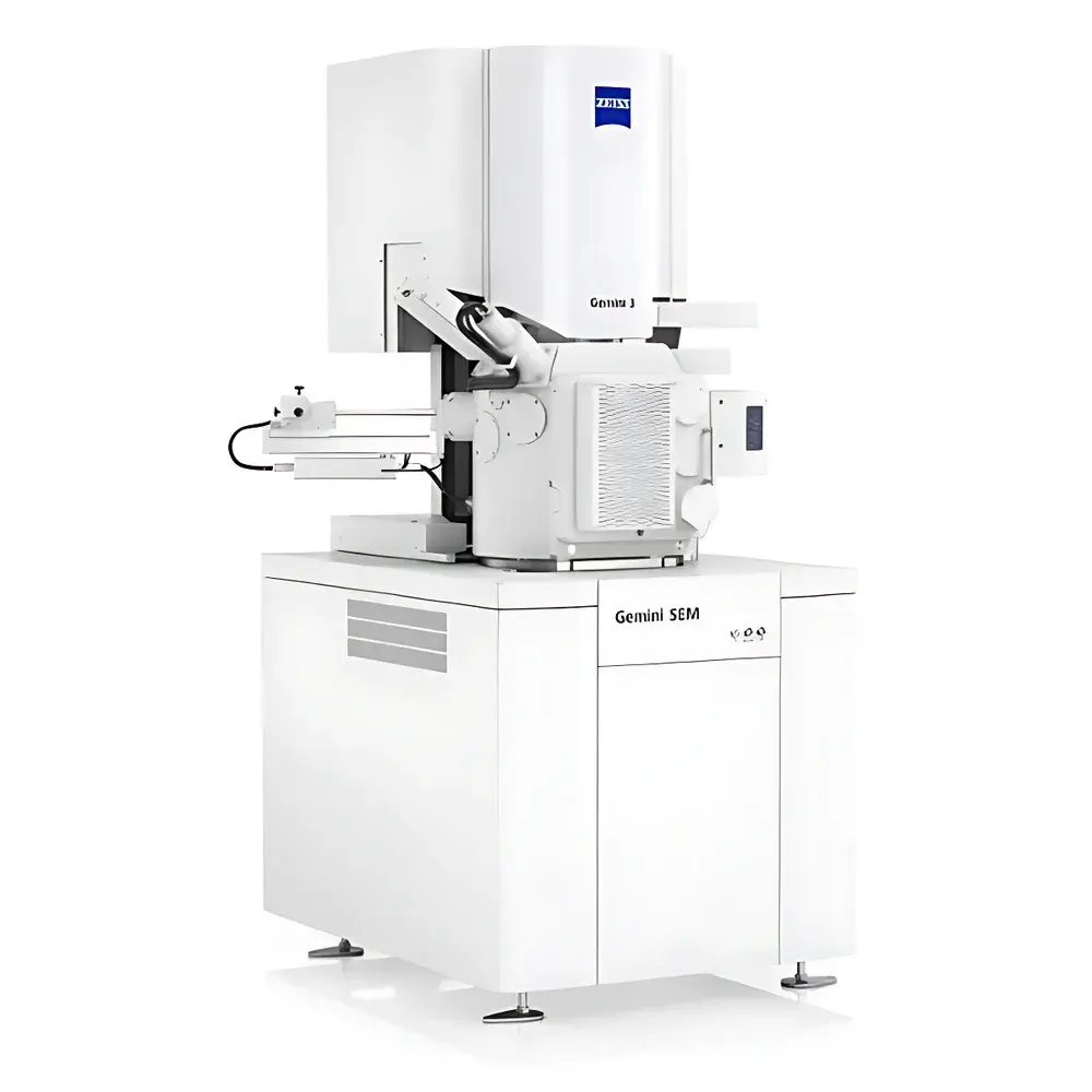
ZEISS GeminiSEM Field Emission Scanning Electron Microscope
| Brand | ZEISS |
|---|---|
| Origin | Shanghai, China |
| Manufacturer Type | Original Equipment Manufacturer (OEM) |
| Country of Origin | China |
| Model | GeminiSEM |
| Instrument Form Factor | Floor-standing |
| Electron Source | Thermal Field Emission Gun (TFEG) |
| Pricing | Upon Request |
Overview
The ZEISS GeminiSEM is a high-performance field emission scanning electron microscope engineered for demanding industrial and academic research environments. Leveraging ZEISS’s proprietary Gemini electron optical column—featuring an in-lens Schottky thermal field emission gun (TFEG) and symmetrical beam path design—the system delivers exceptional signal-to-noise ratio, sub-nanometer resolution at low accelerating voltages (≤1 kV), and high-current stability for quantitative microanalysis. Its large-chamber architecture accommodates samples up to 300 mm in diameter and 150 mm in height, enabling direct examination of full-scale components without sectioning. The column integrates electrostatic and electromagnetic lens hybrid focusing, minimizing chromatic aberration and supporting simultaneous high-resolution imaging and spectroscopic acquisition.
Key Features
- Thermal field emission electron source providing stable probe currents from 0.1 pA to >20 nA, optimized for both high-resolution imaging and high-throughput elemental mapping
- Dual symmetric EDS ports positioned at ±35° relative to the sample surface, enabling high-collection-efficiency energy-dispersive X-ray spectroscopy with minimal shadowing effects
- Co-planar EDS/EBSD integration—both detectors mounted on the same horizontal plane—ensuring precise spatial correlation between compositional and crystallographic data
- Large-volume specimen chamber (Ø 300 mm × H 150 mm) with motorized 5-axis stage (X/Y/Z/tilt/rotation), supporting in situ mechanical testing and heating stages up to 1200 °C
- SmartScan™ acquisition engine with real-time drift correction and adaptive dwell time optimization for artifact-free, high-fidelity mapping at scan speeds up to 60 fps (at 1024 × 768)
- Integrated vacuum architecture with differential pumping stages and ion getter pump, maintaining <2 × 10⁻⁷ mbar in the column during operation
Sample Compatibility & Compliance
The GeminiSEM supports conductive, semi-conductive, and insulating specimens—including ceramics, polymers, composites, and metallurgical cross-sections—without mandatory metal coating, thanks to its low-voltage imaging capability and beam deceleration mode. Sample handling complies with ISO 14644-1 Class 5 cleanroom protocols during chamber loading. All hardware and software modules are designed to meet IEC 61000-6-3 (EMC) and IEC 61000-6-2 (immunity) standards. For regulated environments, optional audit trail logging, user access control tiers, and electronic signature support align with FDA 21 CFR Part 11 and EU Annex 11 requirements when deployed under validated GLP/GMP workflows.
Software & Data Management
Acquisition and analysis are managed through ZEISS SMART-SEM software—a modular platform supporting automated workflow scripting (Python API), batch processing, and multi-instrument synchronization. Image metadata is embedded in TIFF/DM3 formats compliant with ASTM E1558–22 (digital image data exchange). Quantitative EDS maps are processed using AZtec Engine with standardless quantification (based on Cliff-Lorimer and ZAF corrections), traceable to NIST SRM reference materials. Raw data and processed results are exportable in HDF5 format for integration into LIMS or enterprise data lakes. Software updates follow ZEISS’s cybersecurity policy, with annual penetration testing and CVE vulnerability patching aligned with ISO/IEC 27001.
Applications
- Failure analysis of MEMS devices, solder joints, and PCB interconnects—identifying voids, Kirkendall porosity, and intermetallic growth via backscattered electron (BSE) contrast and line-scan EDS
- Fractography and metallurgical evaluation—including cleavage vs. ductile fracture mode differentiation, grain boundary segregation mapping, and phase identification via EBSD pattern indexing
- Microstructure characterization of additive-manufactured alloys, battery cathode particles, and catalyst supports—resolving pore networks, secondary phases, and lattice strain gradients
- Contamination forensics—localizing and chemically fingerprinting sub-micron particulates (e.g., SiO₂, Al₂O₃, Fe-rich oxides) on semiconductor wafers or optical coatings
- In situ dynamic experiments—coupling mechanical loading (via Hysitron PI95 holder) or thermal cycling (Kammrath & Weiss HTS stage) with synchronized SEM/EDS/EBSD data capture
FAQ
What vacuum level does the GeminiSEM maintain in the electron column during operation?
The column operates at ≤2 × 10⁻⁷ mbar, sustained by a combination of turbomolecular and ion getter pumps with active pressure monitoring.
Is the system compatible with third-party EBSD detectors?
Yes—the co-planar port geometry and standardized detector interface (USB 3.0 + LVDS) support OEM EBSD systems from Oxford Instruments, EDAX, and Bruker.
Can the GeminiSEM perform automated particle analysis on irregular bulk samples?
Yes—using ParticleMetric module, it executes morphology-based classification (size, aspect ratio, convexity) across stitched mosaics up to 100 mm², with configurable thresholding and statistical reporting per ISO 13322-1.
Does ZEISS provide application-specific validation documentation?
Yes—method qualification packages (including resolution verification per ISO 16700, EDS accuracy per ASTM E1508, and repeatability studies) are available upon request for GxP-regulated labs.
How is thermal drift compensated during long-duration EBSD mapping?
The system applies real-time stage position feedback via integrated capacitive encoders and performs periodic recalibration of pattern center coordinates using dynamic reference indexing.


