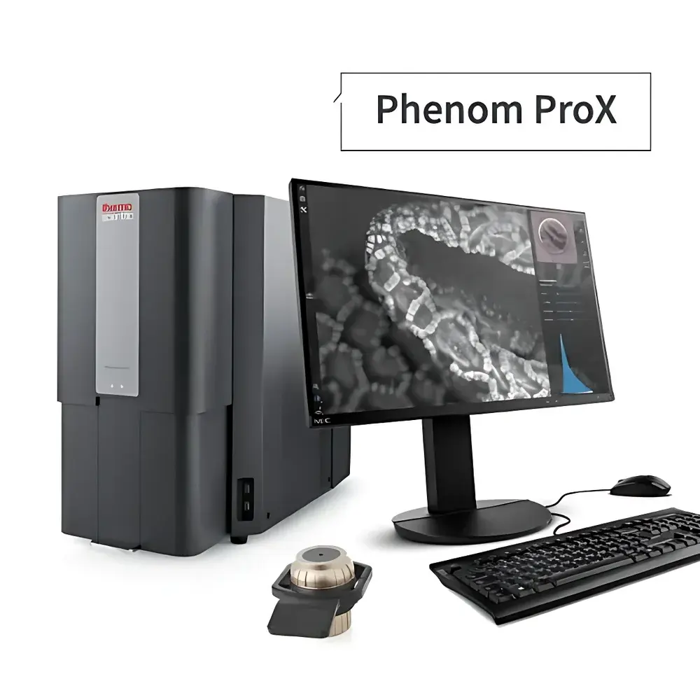
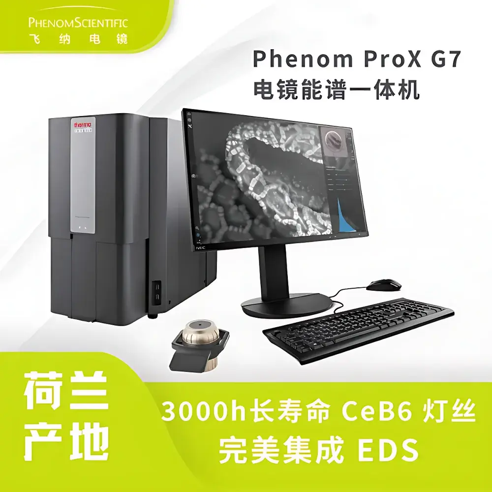
Phenom ProX Desktop SEM-EDS Integrated System
| Brand | Phenom |
|---|---|
| Origin | Netherlands |
| Model | Phenom ProX SEM-EDS Integrated System |
| Instrument Type | Desktop Scanning Electron Microscope |
| Electron Source | CeB6 (Cerium Hexaboride) |
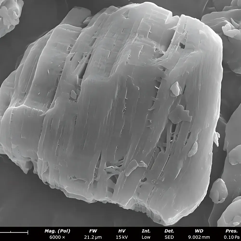
| Secondary Electron Resolution | 6 nm |
| Maximum Magnification | 350,000× |
| Accelerating Voltage | Basic modes: 2 kV, 5 kV, 10 kV, 15 kV, 20 kV |
| Advanced mode | continuously adjustable from 4.8 kV to 20.5 kV |
| Backscattered Electron Resolution | 6 nm |
| Standard Detector | High-sensitivity quadrant backscattered electron detector (BSE) with compositional and topographic imaging modes |
| Optional Detector | Secondary Electron Detector (SED), Mix mode imaging with adjustable SE/BSE ratio |
| EDS Detector | Silicon Drift Detector (SDD) |
| EDS Cooling | Peltier thermoelectric cooling (liquid-nitrogen-free) |
| Elemental Range | Boron (Z=5) to Americium (Z=95) |
| Vacuum Pump-down Time | <15 s |
| Filament Lifetime | ~3,000 hours |
| Optical Zoom | 20×–135× |
| Environmental Tolerance | No anti-vibration table required |
Overview
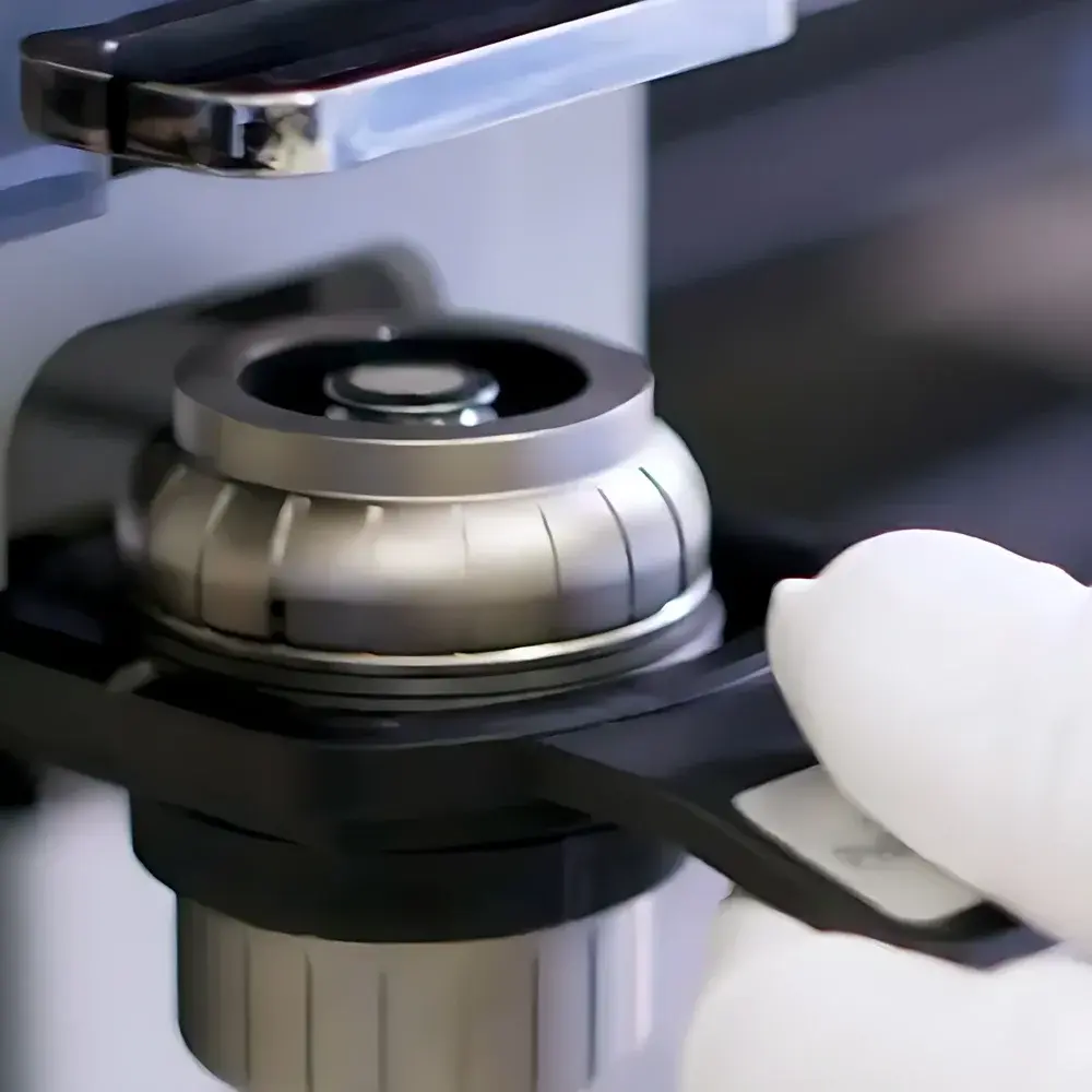
The Phenom ProX Desktop SEM-EDS Integrated System is a fully engineered, factory-aligned scanning electron microscope (SEM) combined with an energy-dispersive X-ray spectroscopy (EDS) module in a single compact platform. Unlike modular add-on configurations, the Phenom ProX integrates beam generation, signal detection, vacuum architecture, and spectral acquisition at the manufacturing stage—ensuring optimal alignment between electron optics and EDS geometry for high spatial correlation between morphology and composition. It employs a thermionic CeB6 electron source delivering 10× higher brightness than conventional tungsten filaments, enabling stable high-resolution imaging at low accelerating voltages (down to 2 kV) while maintaining sufficient beam current for quantitative elemental mapping. The system operates on a robust, sealed-column design with a turbomolecular pumping system achieving full operational vacuum in under 15 seconds—eliminating the need for cryogenic cooling, external chiller units, or dedicated vibration-isolated floors. This architecture supports routine use in shared laboratories, quality control environments, and production floor settings where space, infrastructure, and operational simplicity are critical constraints.
Key Features
- Integrated SEM-EDS platform with co-registered imaging and microanalysis—no post-acquisition alignment required
- CeB6 electron source with >3,000-hour lifetime and consistent emission stability across voltage ranges
- Dual-mode BSE detector: quadrant configuration enables simultaneous topographic and atomic-number contrast imaging
- Optional SED for enhanced surface detail at low kV, with real-time Mix mode blending of SE and BSE signals
- Peltier-cooled SDD detector covering elemental range from B (Z=5) to Am (Z=95); no liquid nitrogen handling or refills
- Accelerating voltage continuously adjustable from 4.8 kV to 20.5 kV in advanced mode—optimized for both high-resolution imaging and peak separation in EDS spectra
- Automated workflows including one-click vacuum initiation, auto-focus, auto-stigmation, and drift-compensated stage navigation
- Optical navigation camera (20×–135×) integrated into the column for rapid region-of-interest selection and correlative optical-SEM analysis
Sample Compatibility & Compliance
The Phenom ProX accommodates a broad range of conductive and non-conductive specimens without mandatory sputter coating—including polymers, ceramics, biological tissues, and insulating powders—thanks to its low-kV imaging capability and charge compensation via beam-induced surface conduction. Sample chambers accept standard 100 mm diameter stubs and optional multi-position holders for high-throughput batch analysis. All hardware and software components comply with IEC 61000-6-3 (EMC emissions) and IEC 61000-6-2 (immunity) standards. The EDS data acquisition and reporting modules support audit trails, user authentication, and electronic signature functionality aligned with FDA 21 CFR Part 11 requirements when deployed in regulated environments such as GLP or GMP-compliant labs. Routine calibration verification follows ISO 16700 (microanalysis of particulate matter) and ASTM E1508 (quantitative elemental analysis by EDS).
Software & Data Management
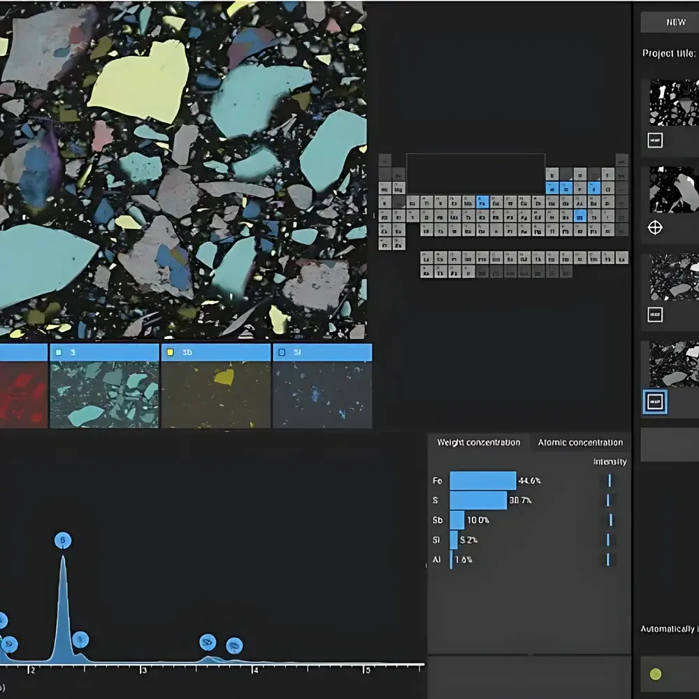
Operation is managed through Phenom Desktop Software—a unified interface for SEM imaging, EDS spectrum acquisition, point/line/area analysis, and automated report generation. The software includes embedded spectral deconvolution algorithms compliant with the ZAF and φ(ρz) matrix correction models. Data files are stored in vendor-neutral HDF5 format, supporting metadata embedding per ISO/IEC 11179 for traceability. Batch processing scripts enable reproducible workflows for particle sizing, phase identification, inclusion counting, fiber length distribution, and 3D surface roughness reconstruction—all validated against NIST SRM reference materials. Remote access, multi-user role management, and integration with LIMS via RESTful API ensure scalability across centralized core facilities and distributed R&D networks.
Applications
The Phenom ProX serves as a primary characterization tool in academic materials science departments, battery R&D labs (cathode/anode morphology and transition metal distribution), semiconductor failure analysis (interconnect voiding, solder joint integrity), metallurgical QC (inclusion analysis per ASTM E45), geoscience (mineral phase mapping), and pharmaceutical solid-state characterization (API crystallinity and excipient dispersion). Its rapid turnaround time (<90 s from load to first image + spectrum) makes it suitable for in-line process monitoring and root-cause investigation in lean manufacturing environments. The system’s repeatability—demonstrated in inter-laboratory round-robin studies—supports ISO/IEC 17025 accreditation pathways for accredited testing laboratories.
FAQ
Does the Phenom ProX require liquid nitrogen for EDS operation?
No. The integrated SDD detector uses Peltier thermoelectric cooling and operates continuously without cryogen refills.
Can non-conductive samples be imaged without sputter coating?
Yes. Low-kV imaging (2–5 kV) combined with BSE signal optimization enables high-fidelity imaging of uncoated polymers, ceramics, and biological specimens.
What is the typical maintenance interval for the CeB6 source?
Filament replacement is recommended after approximately 3,000 hours of cumulative beam-on time, with minimal downtime and no realignment required.
Is the system compatible with regulatory documentation requirements?
Yes. Audit trail logging, user access controls, and electronic signature support meet FDA 21 CFR Part 11 and EU Annex 11 criteria for validated analytical environments.
How is spatial registration between SEM images and EDS maps ensured?
The EDS detector is mechanically fixed relative to the electron column, and all acquisitions share identical stage coordinates and magnification calibration—eliminating pixel-shift artifacts common in retrofit systems.


