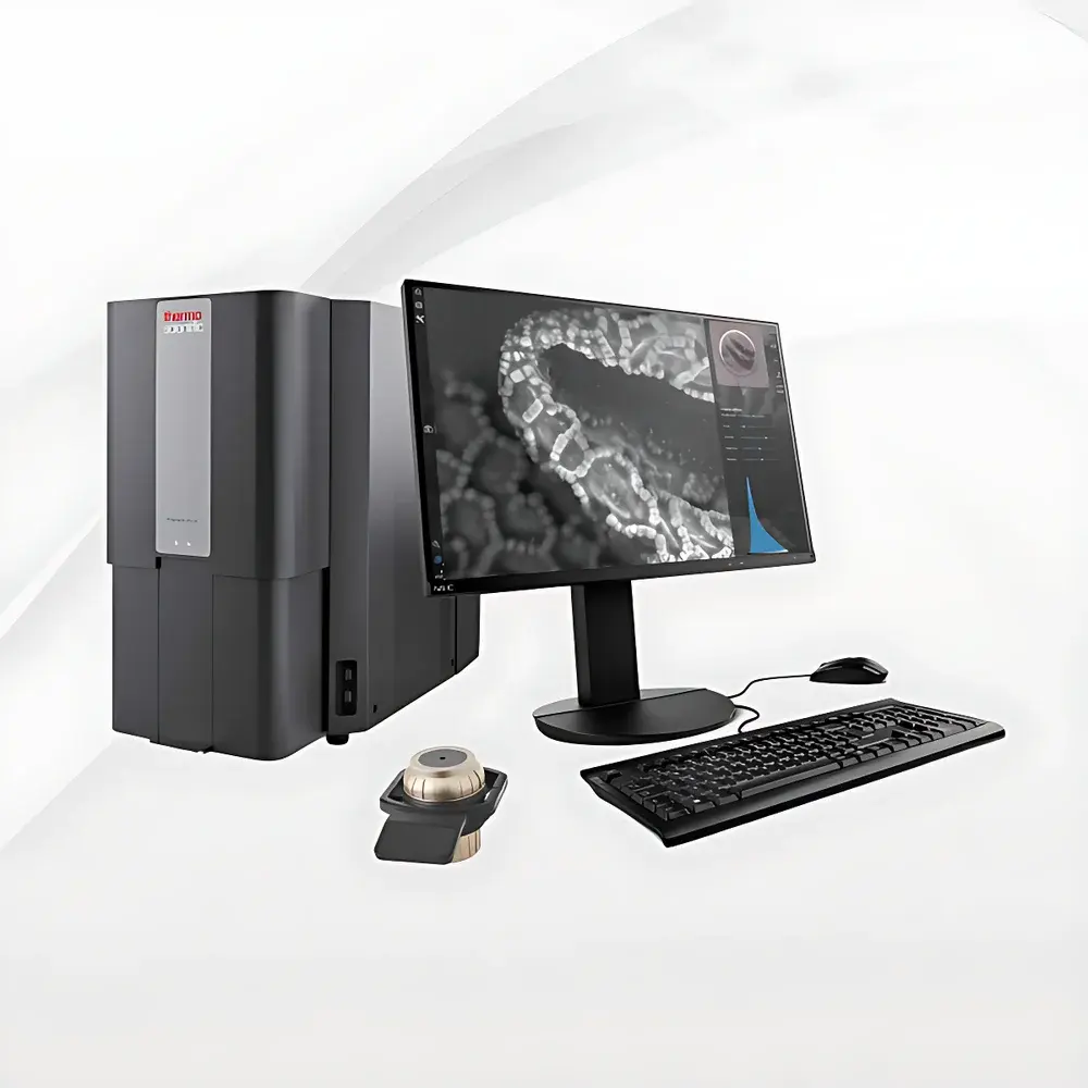
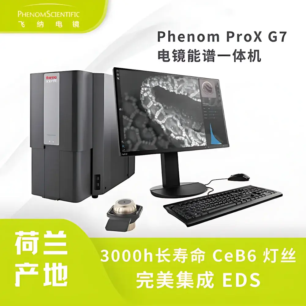
Phenom ProX Desktop Scanning Electron Microscope with Integrated EDS
| Brand | Phenom |
|---|---|
| Origin | Netherlands |
| Model | ProX |
| Instrument Type | Desktop SEM |
| Electron Source | CeB6 (Cerium Hexaboride) |
| Secondary Electron Resolution | 6 nm |
| Maximum Magnification | 350,000× |
| Accelerating Voltage Range | 4.8–20.5 kV |
| Backscattered Electron Resolution | 6 nm |
| EDS Detector | Silicon Drift Detector (SDD) |
| Cooling | Peltier (liquid-nitrogen-free) |
| Vacuum Pump-down Time | <15 s |
| Elemental Analysis Range | B (5) to Am (95) |
| Operating Environment | Standard lab/office/facility (no anti-vibration table required) |
Overview
The Phenom ProX Desktop Scanning Electron Microscope with Integrated EDS is a fully engineered, factory-aligned SEM-EDS platform designed for rapid, high-fidelity surface imaging and quantitative elemental characterization in non-dedicated laboratory spaces. Unlike conventional floor-standing SEMs requiring dedicated infrastructure, the ProX employs a robust, compact architecture centered on a high-brightness CeB6 thermionic electron source—delivering 10× greater brightness than standard tungsten filaments—enabling stable imaging at low accelerating voltages (down to 2 kV) while maintaining sub-6 nm resolution at 10 kV. Its integrated scanning electron optics operate on a dual-beam principle: secondary electrons (SE) for topographic contrast and backscattered electrons (BSE) for atomic number (Z)-contrast imaging. Coupled directly to a high-efficiency silicon drift detector (SDD), the system performs simultaneous or sequential microstructural observation and energy-dispersive X-ray spectroscopy (EDS) without mechanical reconfiguration. This seamless hardware integration eliminates calibration drift between imaging and analysis modes—a critical advantage for reproducible, GLP-compliant workflows in regulated environments.
Key Features
- Sub-6 nm resolution at 10 kV, validated per ISO 16700:2016 for SEM resolution measurement
- CeB6 electron source with >3,000-hour operational lifetime and auto-alignment capability
- Full vacuum cycle completed in under 15 seconds using a turbomolecular pump and dry scroll backing pump
- No cryogenic cooling required: Peltier-cooled SDD detector ensures continuous EDS operation without liquid nitrogen logistics
- Integrated four-quadrant BSE detector enabling compositional contrast, phase mapping, and topographic shading in real time
- Automated stage navigation, autofocus, and astigmatism correction reduce operator dependency and accelerate routine analysis
- Non-conductive sample compatibility via low-kV imaging (2–5 kV) and charge compensation mode—eliminating mandatory sputter coating for most insulators
- Modular software architecture supporting optional certified modules: ParticleMetric (ASTM E2947-compliant particle analysis), FiberMetric (ISO 9277-based fiber sizing), and MetalInclusion (EN 10247-compliant inclusion rating)
Sample Compatibility & Compliance
The Phenom ProX accommodates a broad range of solid, dry, and heterogeneous specimens—including battery cathode/anode powders, sintered metal alloys, semiconductor wafers, geological thin sections, and polymer composites—without size limitation beyond the standard 100 mm diameter stage. Samples are loaded manually into standardized sample cups (available in conductive, non-conductive, and grid-mounted variants), enabling rapid exchange and traceable positioning. The system complies with IEC 61000-6-3 (EMC emissions) and IEC 61000-6-2 (immunity), and its EDS quantification engine supports ZAF and φ(ρz) matrix corrections per ISO 14704:2021 for bulk and thin-film analysis. Full audit trail logging, user access controls, and electronic signature support align with FDA 21 CFR Part 11 requirements when configured with validated software packages.
Software & Data Management
Operation is unified within Phenom Desktop Software v6.x—a Windows-based application featuring intuitive ribbon interface, scriptable automation (via Python API), and native DICOM/ TIFF/EDAX .emsa export. All imaging and EDS data—including spectra, maps, and quantification reports—are stored in a self-contained project file (.phenom) with embedded metadata (operator ID, timestamp, instrument configuration, vacuum history). Spectral processing uses real-time deconvolution (based on the Sherman equation) and peak identification against the NIST Standard Reference Database (SRD 107). Batch analysis workflows support automated report generation compliant with ISO/IEC 17025 documentation standards, including uncertainty estimation per GUM (JCGM 100:2008). Raw EDS spectra and map datasets are exportable in standard formats (e.g., .spc, .tdf, .hdf5) for third-party validation or machine learning preprocessing.
Applications
The Phenom ProX serves as a primary analytical tool across academic, industrial, and regulatory laboratories. In battery R&D, it enables in-situ monitoring of cathode cracking, SEI layer thickness estimation (via cross-section imaging), and transition-metal leaching quantification via line scans. In metallurgy, it supports ASTM E112 grain size analysis, EN 10247 non-metallic inclusion classification, and porosity distribution mapping in additive-manufactured components. Semiconductor failure analysts utilize its high-resolution BSE imaging to localize voids, delamination, or Cu diffusion in BEOL structures. Geological labs apply its automated mineral identification (using spectral library matching against RRUFF and Mindat databases) for petrographic quantification. Within shared instrumentation facilities, its plug-and-play deployment, minimal footprint (<0.5 m²), and guided workflow reduce training time from weeks to hours—making it ideal for multi-user, high-throughput environments.
FAQ
Does the Phenom ProX require external vibration isolation?
No. Its monolithic column design and active damping system meet ISO 25317:2016 stability criteria for desktop SEMs, allowing installation on standard laboratory benches.
Can EDS analysis be performed without prior SEM imaging?
Yes. The system supports direct point-and-shoot EDS acquisition using optical microscope guidance (20–135×) or coordinate-based stage positioning.
Is the CeB6 filament user-replaceable?
Yes. Filament replacement is a field-service procedure requiring no realignment; typical interval is 5 years under average usage (≈1 h/day).
What standards does the EDS quantification follow?
Quantitative results adhere to ISO 14704:2021 (microanalysis by EDS) and include k-ratio calculation, matrix correction, and detection limit reporting per IUPAC guidelines.
How is data integrity ensured during long-duration mapping?
The software implements real-time drift correction using fiducial markers and logs all instrumental parameters (beam current, dwell time, live time) with each pixel—ensuring full traceability for ISO/IEC 17025 audits.