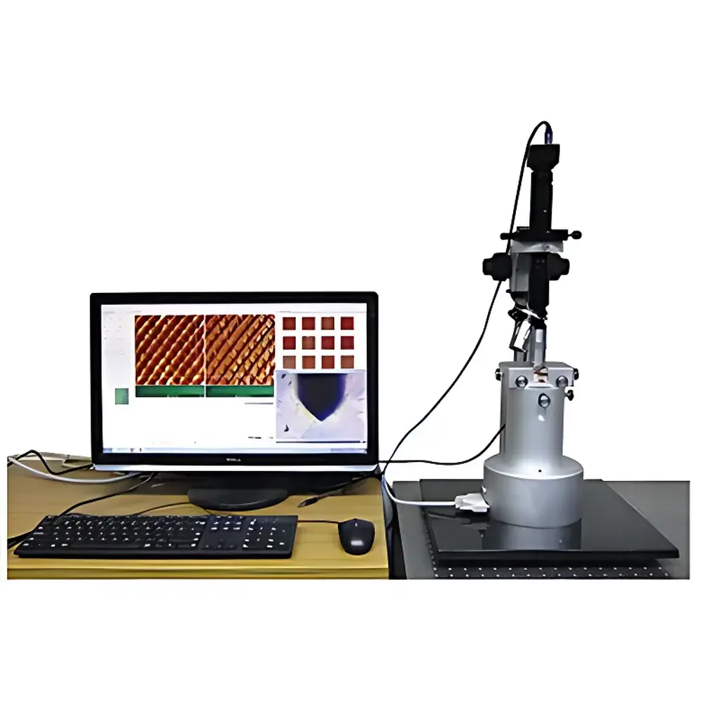
Betop Scientific CSPM6000 Hybrid Optical-AFM Integrated Microscope
| Brand | Betop Scientific |
|---|---|
| Origin | Guangdong, China |
| Manufacturer Type | OEM Manufacturer |
| Country of Origin | China |
| Model | CSPM6000 |
| Instrument Type | Atomic Force Microscope (AFM) |
| Position Detection Noise | ≤0.1 nm |
| Sample Dimensions | Ø < 100 mm, Thickness < 40 mm |
| XY Sample Stage Travel Range | 100 mm × 100 mm |
| Force Sensitivity | ≤5 pN |
| Image Resolution Options | 128×128 to 4096×4096 pixels |
| Scan Rotation | 0–360° |
| Scan Frequency Range | 0.1–100 Hz |
| Control Architecture | Dual-core DSP+ARM processor (Texas Instruments) |
| Feedback System | Fully digital PID-controlled feedback with auto-tuning |
| Communication Interfaces | Gigabit Ethernet (TCP/IP) + High-Speed USB 2.0 |
| Display | 16×4 LCD with real-time system diagnostics |
| Software | Multi-language (EN/CN-Traditional/CN-Simplified), Windows 10/7/XP/Vista compatible |
Overview
The Betop Scientific CSPM6000 is a hybrid optical–atomic force microscope (Optical-AFM) platform engineered for correlative nanoscale imaging and quantitative surface characterization in research and industrial quality control environments. It integrates a high-stability upright optical microscope with a precision scanning probe module based on piezoelectric tube actuation and optical beam deflection (OBD) detection—enabling simultaneous topographic, mechanical, electrical, and optical interrogation of solid-state samples under ambient or controlled environmental conditions. The system operates on the fundamental principle of detecting cantilever deflection induced by tip–sample interatomic forces, with sub-nanometer vertical resolution (≤0.03 nm RMS) and lateral resolution down to 0.2 nm. Its modular architecture supports both contact-mode and dynamic-mode AFM (tapping, phase imaging, amplitude modulation), as well as advanced functional extensions including lateral force microscopy (LFM), conductive AFM (C-AFM), magnetic force microscopy (MFM), electrostatic force microscopy (EFM), liquid-cell AFM, and nanomechanical mapping (nanoindentation, vector patterning). Designed for reproducibility and long-term stability, the CSPM6000 complies with ISO/IEC 17025-relevant calibration traceability practices and supports GLP/GMP-aligned data integrity workflows.
Key Features
- Co-registered optical and AFM imaging via a flat-optic probe head design, enabling real-time visual navigation and region-of-interest targeting without sample repositioning
- Dual-resolution scanning capability: interchangeable 1.5 µm × 1.5 µm and 15 µm × 15 µm piezoscanners optimized for high-resolution nanostructure analysis and large-area survey mapping
- Embedded dual-core TI DSP+ARM controller with fully digital, adaptive PID feedback—eliminating manual tuning and ensuring consistent loop response across varying sample stiffness and environmental drift
- Open-architecture I/O interface compliant with standard D-sub connector pinouts (Power, AD/DA, DI/DO, Signal In/Out), supporting third-party signal modulation, external stimulus synchronization (e.g., voltage bias, thermal ramping), and hardware-in-the-loop experimentation
- Gigabit Ethernet and USB 2.0 dual-communication protocol ensures deterministic timing accuracy (<100 µs jitter) for time-resolved measurements such as force spectroscopy, creep relaxation, or dynamic mechanical analysis
- Real-time 3D surface rendering engine with multi-channel overlay (topography, phase, friction, current, etc.), adjustable pseudo-color LUTs (24-bit customizable palettes), and live contrast/brightness optimization
Sample Compatibility & Compliance
The CSPM6000 accommodates standard wafer- and substrate-mounted specimens up to Ø100 mm and 40 mm thick, including silicon wafers, glass slides, metal foils, polymer films, biological membranes (on mica or SiO₂), and electrochemical electrodes. Magnetic and non-magnetic sample holders (Ø12.5 mm, 1.5 mm thick) are included for flexible mounting. The instrument’s mechanical isolation design minimizes acoustic and vibrational coupling, meeting ISO 25178-6 requirements for vibration-sensitive metrology. All software modules adhere to FDA 21 CFR Part 11 principles for electronic records and signatures, including audit trails, user access controls, and immutable raw-data export (ASCII, TIFF, HDF5). Calibration artifacts and traceable reference standards (e.g., NIST SRM 1960, 2000) are supported through documented procedures aligned with ISO/IEC 17025 clause 6.6.
Software & Data Management
The CSPM6000 ships with Betop’s proprietary “NanoControl Suite”, comprising two integrated applications: NanoControl (real-time acquisition and instrument control) and NanoAnalyze (post-processing and quantitative analysis). Both support English, Simplified Chinese, and Traditional Chinese UIs and run natively on Windows 10 (64-bit), Windows 7 SP1+, and legacy OS versions via compatibility mode. NanoControl features scriptable vector scanning, tip-shape deconvolution algorithms, automatic image reconstruction, and synchronized multi-parameter acquisition (e.g., topography + current + phase at 1024×1024 @ 2 Hz). NanoAnalyze provides over 30 built-in filters—including Gaussian, median, rolling-ball, TOP-HAT, and local-statistics-based line removal—as well as cross-sectional profiling, roughness statistics (Sa, Sq, Sz per ISO 25178-2), grain analysis, and batch processing macros. Raw data exports retain full metadata (scan parameters, timestamp, PID gains, sensor calibration coefficients) in open formats for third-party interoperability.
Applications
- Nanomaterial characterization: graphene layer counting, CNT dispersion analysis, MOF surface morphology, quantum dot size distribution
- Semiconductor metrology: gate oxide thickness uniformity, trench profile asymmetry, CMP defect mapping
- Biophysics: amyloid fibril mechanics, lipid bilayer elasticity, protein unfolding kinetics via force–distance spectroscopy
- Energy materials: SEI layer evolution on Li-ion battery anodes, catalyst nanoparticle sintering behavior, perovskite film grain boundary conductivity
- Polymer science: phase separation in block copolymers, nanocomposite filler dispersion, viscoelastic mapping via amplitude-modulated AFM
- Nanofabrication process development: lithographic pattern fidelity assessment, nanoimprint residual layer thickness, etch depth uniformity
FAQ
Does the CSPM6000 support liquid-phase AFM?
Yes—the system includes a fluid cell accessory kit compatible with aqueous and organic solvents, enabling in situ electrochemical AFM, biomolecular interaction studies, and corrosion monitoring.
Can the optical microscope be used independently of the AFM module?
Yes—the upright optical path is mechanically decoupled and fully functional as a standalone brightfield/darkfield microscope with 10×–100× objectives and LED illumination.
Is third-party probe compatibility guaranteed?
The CSPM6000 accepts standard 12.7 mm × 3.0 mm rectangular AFM probes from major vendors (Bruker, Nanoworld, Olympus); however, optimal performance requires calibration of photodiode sensitivity and laser alignment for each new probe type.
What level of technical support and training is provided?
Betop Scientific offers remote commissioning, on-site installation (optional), and comprehensive operator certification programs covering instrument operation, maintenance, calibration, and ISO-compliant reporting.
Are software updates and firmware patches available post-purchase?
Yes—customers receive free minor version updates and security patches for five years; major releases are available under optional annual software maintenance agreements.