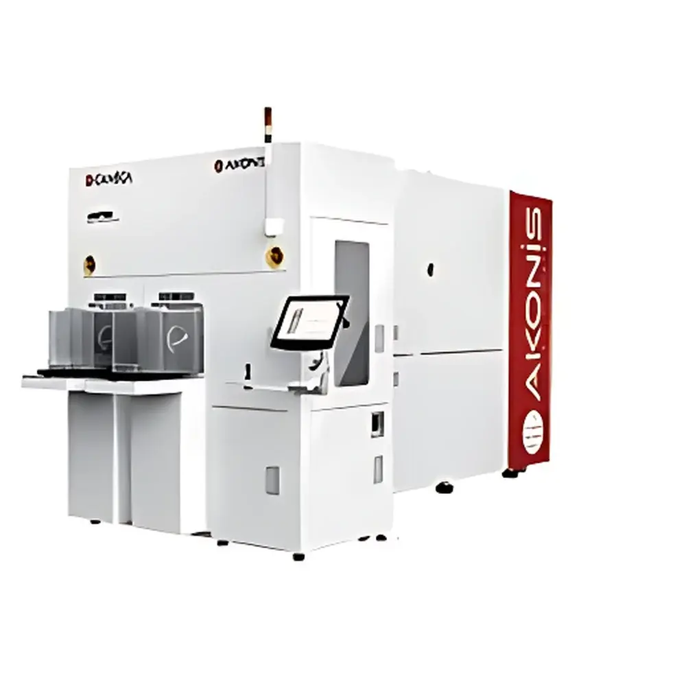
CAMECA AKONIS Fully Automated In-Line Secondary Ion Mass Spectrometer
| Brand | Cameca |
|---|---|
| Origin | France |
| Model | AKONIS |
| Instrument Type | Magnetic Sector SIMS |
| Certification | SEMI S2/S8, E4, E5, E39, E84 Compliant |
| Automation Level | Full In-Line Integration |
| Minimum Measurement Spot Size | 20 µm |
| Positioning Accuracy | < 2 µm |
| Primary Ion Energy Range | < 150 eV (EXLIE Column) |
| Wafer Handling | Full-Size Patterned & Blank Wafer Compatible |
| Cost of Ownership | Optimized for High-Volume Semiconductor Fab Deployment |
| Regulatory Alignment | Designed for GLP/GMP-aligned process control environments |
Overview
The CAMECA AKONIS is a fully automated, in-line secondary ion mass spectrometer engineered specifically for high-throughput compositional metrology in advanced semiconductor fabrication facilities. Unlike conventional laboratory-based SIMS systems—such as the IMS Wf/SC Ultra or SIMS 4550 quadrupole platforms—the AKONIS integrates directly into cleanroom production workflows, delivering real-time, high-fidelity depth profiling and dopant quantification without compromising analytical sensitivity. Its core architecture leverages magnetic sector mass analysis, enabling superior mass resolution and isotopic fidelity essential for sub-nanometer interface characterization in SiGe, SiP, and multi-layer heterostructure devices. The system employs CAMECA’s proprietary EXLIE (Extra-Low Impact Energy) primary ion column, operating below 150 eV to minimize sputter-induced mixing while preserving atomic-scale depth resolution—critical for N5 and beyond technology nodes. Designed from the ground up for 300 mm wafer compatibility, AKONIS supports both blanket and patterned wafers, with automated pattern recognition and interferometric stage positioning ensuring repeatable < 2 µm spatial registration across full-wafer maps.
Key Features
- Fully automated in-line integration compliant with SEMI standards (S2/S8, E4, E5, E39, E84), enabling seamless deployment in Class 10 cleanrooms without dedicated lab infrastructure.
- EXLIE ion optics delivering primary beam energies < 150 eV—reducing atomic redistribution during sputtering and enhancing depth resolution for ultra-shallow junctions and interfacial layers.
- 20 µm minimum analysis spot size optimized for bond pad and test structure interrogation, supporting rapid feedback loops with >97% reduction in time-to-data versus off-line lab analysis.
- High-precision interferometric XY stage coupled with AI-assisted pattern recognition engine for sub-2 µm positional repeatability on patterned wafers—even under dynamic fab environmental conditions.
- Intuitive recipe editor powered by CAMECA’s proprietary materials database, allowing process engineers to define acquisition protocols without SIMS expertise; all parameters traceable and version-controlled.
- Robust magnetic sector mass analyzer providing stable mass calibration over extended run times, supporting long-term reproducibility required for statistical process control (SPC) and tool-to-tool matching.
Sample Compatibility & Compliance
AKONIS is qualified for direct integration into front-end-of-line (FEOL) and back-end-of-line (BEOL) process control lines handling silicon, SiGe, GaN, and advanced packaging substrates. It accommodates standard 300 mm wafers—including those with topography, dielectric stacks, and metal interconnects—without manual intervention. All safety, emissions, and electrical compliance documentation conforms to SEMI S2 (safety guidelines), S8 (ergonomics), E4 (EMC), E5 (electrical safety), E39 (cleanroom compatibility), and E84 (software lifecycle management). The platform supports audit-ready data integrity per FDA 21 CFR Part 11 requirements, including electronic signatures, change control logs, and immutable audit trails for all acquisition and calibration events.
Software & Data Management
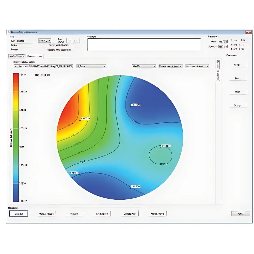
The AKONIS Control Suite provides a unified interface for method development, real-time monitoring, and automated reporting. Acquisition sequences are defined via structured recipes that enforce parameter constraints and cross-check against material-specific calibration libraries. Raw spectral data are stored in vendor-neutral HDF5 format with embedded metadata (instrument configuration, vacuum status, beam current, stage coordinates). Integrated data reduction modules support ISO/IEC 17025-compliant quantification using matrix-matched standards and relative sensitivity factors (RSFs). Export options include CSV, XML, and direct API integration with factory MES and APC systems. All software updates follow IEC 62304-compliant development lifecycle protocols, with full validation documentation available for GMP audits.
Applications
- Ultra-shallow junction depth profiling (e.g., B, P, As in sub-5 nm channel regions)
- Interface composition analysis at Si/SiO₂, Si/SiGe, and metal/dielectric boundaries
- Contamination screening for metallic impurities (Fe, Cu, Ni, Na) at ppt-level detection limits
- Strain engineering verification in strained-Si and Ge-on-Si heterostructures
- Process drift detection across multiple tools via automated cross-wafer correlation
- Qualification of ALD/CVD film stoichiometry and interdiffusion kinetics in 3D NAND and DRAM stacks
FAQ
Is AKONIS compatible with existing fab automation infrastructure (SECS/GEM)?
Yes—AKONIS includes native SECS/GEM v5.0 and HSMS communication stacks, enabling bidirectional control and status reporting through standard fab host interfaces.
Does AKONIS require dedicated vibration isolation or special utility conditioning?
No—it meets SEMI E39 requirements for cleanroom floor mounting and operates within standard fab utility envelopes (N₂ purge, 230 VAC ±10%, 50/60 Hz, compressed dry air at 6 bar).
How is calibration maintained across shifts and tool clusters?
Calibration is performed automatically before each wafer run using internal reference standards; all calibration events are timestamped, logged, and subject to configurable review thresholds per ISO 9001 Clause 7.1.5.
Can AKONIS perform quantitative analysis without lab-based standards?
Yes—its embedded RSF library covers >120 elemental combinations across common semiconductor matrices; absolute quantification is traceable to NIST SRMs via CAMECA’s certified reference wafer program.
What level of cybersecurity hardening is implemented?
The system runs a locked-down Linux OS with SELinux enforcement, disabled remote shell access by default, TLS 1.2+ encrypted communications, and quarterly security patching aligned with IEC 62443-3-3.
Related Products