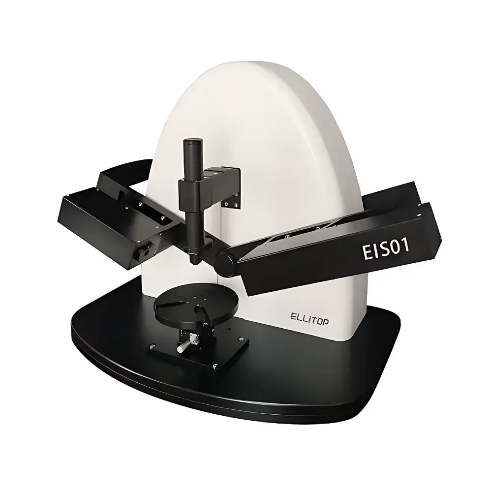
ELLITOP EIS01 Imaging Spectroscopic Ellipsometer
| Brand | ELLITOP |
|---|---|
| Origin | Beijing, China |
| Model | EIS01 |
| Spectral Range (Vis) | 370–1000 nm |
| Incident Angle | Motorized variable from 30° to 90° |
| Single-Wavelength Measurement Time | ~15 s (configuration-dependent) |
| Thickness Repeatability | ±0.05 nm |
| Refractive Index Repeatability | ±0.001 |
Overview
The ELLITOP EIS01 Imaging Spectroscopic Ellipsometer is a precision optical metrology platform engineered for quantitative, spatially resolved characterization of thin films, interfaces, and surface nanostructures. It integrates spectroscopic ellipsometry—the non-contact, model-based optical technique that measures the change in polarization state (Ψ and Δ) of light upon reflection from a sample—with high-magnification microscopic imaging and automated spectral scanning. This fusion enables simultaneous acquisition of ellipsometric parameters (Ψ, Δ), complex dielectric function (ε = ε₁ + iε₂), refractive index (n), extinction coefficient (k), film thickness (d), and absorption coefficient (α) across a defined field of view—without physical contact or sample destruction. Operating across the visible spectrum (370–1000 nm), the EIS01 delivers sub-nanometer vertical sensitivity in thickness determination and micron-scale lateral resolution (down to 1 µm), making it suitable for research and process control in nanofabrication, interfacial science, and functional material development.
Key Features
- Motorized incident angle control (30°–90°) enabling multi-angle spectroscopic acquisition for enhanced parameter decoupling and modeling robustness
- Rotating compensator architecture providing full 0°–360° Δ measurement range with no null-point ambiguity and intrinsic immunity to depolarization effects from surface roughness
- Microscope-coupled optical path supporting real-time visual alignment, region-of-interest (ROI) selection, and high-fidelity spatial mapping
- Broadband achromatic compensation optics ensuring wavelength-independent phase retardation accuracy across the entire spectral range
- Multi-quadrant error correction algorithm minimizing systematic drift and enhancing long-term measurement stability and reproducibility
- Integrated Mueller matrix capability (12 normalized elements) for comprehensive depolarization and anisotropy analysis
- Brewster-angle microscopy mode for label-free, in situ observation of monolayer assemblies at air–liquid and liquid–liquid interfaces
Sample Compatibility & Compliance
The EIS01 supports a wide range of solid and quasi-solid samples including silicon wafers, glass substrates, ITO-coated slides, polymer films, 2D materials (graphene, TMDCs), biosensor chips, and functionalized surfaces. It accommodates standard wafer formats (up to 200 mm) and custom sample holders for irregular geometries. Data acquisition and reporting comply with fundamental principles of ISO/IEC 17025 for testing laboratories; measurement traceability is maintained via factory calibration against NIST-traceable reference standards. Software audit trails, user access controls, and electronic signature support align with GLP and FDA 21 CFR Part 11 requirements for regulated environments where data integrity and instrument qualification are mandatory.
Software & Data Management
The proprietary ELLITOP Analysis Suite provides a unified interface for instrument control, real-time imaging, spectral acquisition, optical modeling (including layered stack fitting, effective medium approximation, and dispersion modeling), and quantitative mapping. All raw and processed datasets—including Ψ(λ, x, y), Δ(λ, x, y), n(λ, x, y), k(λ, x, y), d(x, y), and R/T distributions—are stored in HDF5 format with embedded metadata (wavelength grid, angle, exposure, calibration timestamps). Batch processing, scripting (Python API), and export to industry-standard formats (CSV, TIFF, VTK) enable integration into automated QA/QC workflows and LIMS platforms. Version-controlled project files ensure full reproducibility and facilitate collaborative analysis across distributed teams.
Applications
- Semiconductor process monitoring: thickness uniformity mapping of ALD/CVD-grown dielectrics (SiO₂, HfO₂), gate oxides, and hard masks on patterned wafers
- Biointerface characterization: label-free quantification of protein adsorption kinetics, lipid bilayer formation, and receptor–ligand binding on functionalized sensor surfaces
- 2D materials metrology: layer-counting and strain mapping of exfoliated or CVD-grown graphene, MoS₂, and h-BN via thickness-sensitive ellipsometric contrast
- Photonic device development: dispersion profiling of waveguide claddings, anti-reflection coatings, and plasmonic nanostructures
- Advanced packaging: delamination detection and interfacial quality assessment in chip-on-wafer and fan-out wafer-level packaging stacks
- Soft matter research: in situ observation of Langmuir monolayers, polymer brush swelling, and hydrogel hydration dynamics at fluid interfaces
FAQ
What sample types are compatible with the EIS01?
The system accepts flat, reflective, or semi-transparent substrates including silicon, fused silica, sapphire, ITO glass, and flexible polymer films. Transparent substrates require appropriate backside treatment or use of transmission-mode accessories.
Does the EIS01 support multi-layer optical modeling?
Yes—it includes a built-in optical modeling engine capable of fitting arbitrary multilayer stacks (up to 10 layers) with graded interfaces, roughness layers, and anisotropic media using least-squares minimization and confidence interval estimation.
Can the EIS01 be integrated into a cleanroom or automated fab environment?
The instrument features RS-232, Ethernet, and USB 3.0 connectivity, programmable via SCPI commands and Python SDK, enabling integration with SECS/GEM-compliant host systems and MES platforms.
Is training and application support provided?
ELLITOP offers on-site installation, operator certification, and application-specific method development support, including joint feasibility studies for novel material systems.
How is calibration maintained over time?
The system includes automated daily self-check routines, reference mirror validation protocols, and optional annual recalibration services traceable to national metrology institutes.