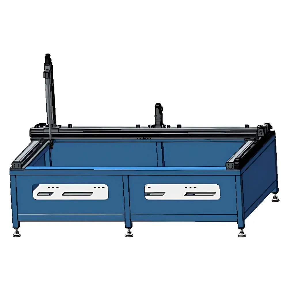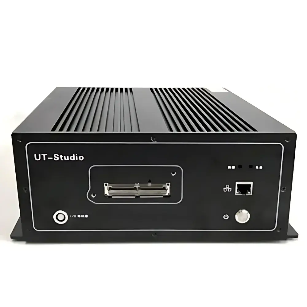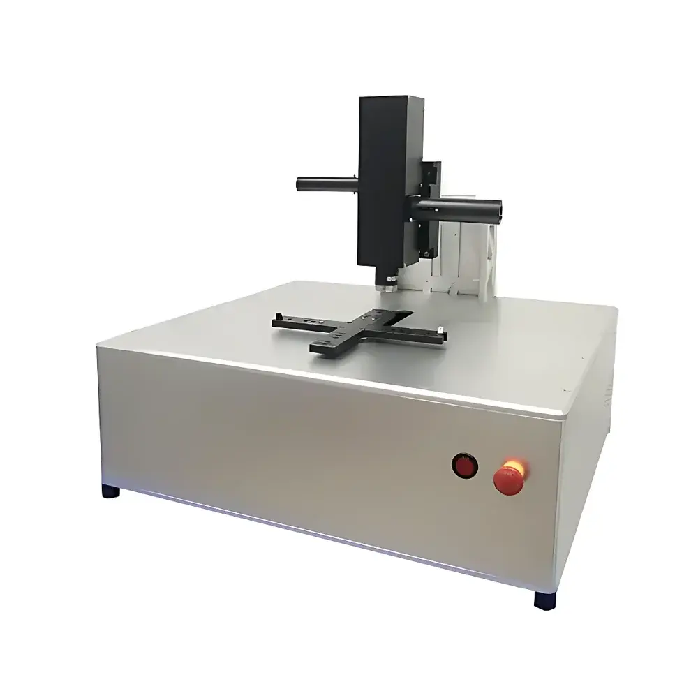
ELLITOP EH200-X White Light Interferometric Thickness Measurement System
| Brand | ELLITOP |
|---|---|
| Model | EH200-X |
| Origin | Beijing, China |
| Wavelength Range | 190–1700 nm |
Overview
The ELLITOP EH200-X is a benchtop white light interferometric thickness measurement system engineered for rapid, non-contact, and label-free characterization of transparent and semi-transparent thin films on reflective substrates. It operates on the physical principle of spectral reflectance interference: a broadband white light beam (190–1700 nm) is directed perpendicularly onto the sample surface via a high-magnification microscope objective. Interference fringes arise from the phase difference between reflections at the air–film and film–substrate interfaces. These fringes are encoded in the wavelength-dependent reflectance spectrum, captured by a high-sensitivity linear CCD spectrometer array. Using inverse optical modeling based on Fresnel equations and rigorous thin-film optics theory, the embedded analysis engine extracts film thickness with nanometer-scale resolution — typically ranging from 300 µm — along with complementary optical constants including refractive index (n) and extinction coefficient (k). The integrated microscope enables spatially resolved micro-area measurements down to ~1 µm lateral resolution, making it suitable for structured surfaces, patterned wafers, and localized process monitoring in R&D and pilot-line environments.
Key Features
- White light interferometry coupled with microscopic imaging for sub-micron spatial resolution
- Single-point measurement completed in under 1 second, enabling high-throughput screening
- Simultaneous extraction of thickness, n(λ), and k(λ) across UV–Vis–NIR (190–1700 nm)
- Optimized for mirror-like substrates (e.g., Si, SiO₂/Si, metal-coated glass, ITO/glass)
- Manual XY stage with coordinate registration for repeatable micro-area targeting
- Standalone operation with intuitive GUI; no external PC or driver installation required
- Rugged mechanical design with thermal drift compensation for stable long-term performance
Sample Compatibility & Compliance
The EH200-X is validated for single-layer and few-layer (≤5 layers) dielectric and organic films on highly reflective planar substrates. Compatible film materials include photoresists (PR), silicon nitride (SiNx), silicon dioxide (SiO₂), aluminum oxide (Al₂O₃), indium tin oxide (ITO), polyimide (PI), PEDOT:PSS, OLED emissive layers (e.g., NPB, Alq₃), and anti-reflective coatings. Substrate flatness should be ≤λ/4 over the measurement area. While not certified to ISO/IEC 17025, the system supports traceable calibration using NIST-traceable SiO₂-on-Si reference wafers. Data acquisition and analysis workflows align with GLP-compliant documentation practices; audit trail logging and user access control can be enabled via optional software modules compliant with FDA 21 CFR Part 11 requirements.
Software & Data Management
The proprietary ELLITOP Thickness Analysis Suite provides real-time spectral fitting, multi-layer optical model construction, and batch processing for map-based data acquisition. Raw spectra, fitted curves, residuals, and parameter confidence intervals are exportable in CSV, TXT, and HDF5 formats. The software supports ASTM E2628-21 (Standard Guide for Spectral Reflectance-Based Thin Film Thickness Measurement) methodology selection and uncertainty estimation per GUM (Guide to the Expression of Uncertainty in Measurement). All measurement metadata — including instrument configuration, environmental conditions (ambient temperature logged), operator ID, and timestamp — are embedded in exported files. Version-controlled software updates ensure backward compatibility with legacy project archives.
Applications
- Semiconductor process control: photoresist spin-coating uniformity, gate dielectric (SiO₂, HfO₂) thickness, etch-stop layer verification
- Flat panel display manufacturing: TFT backplane stack (a-Si, SiNx, ITO), OLED functional layers (HTL, EML, ETL), encapsulation barrier films
- Optical coating QC: AR, HR, and bandpass filter stacks on lenses, mirrors, and laser components
- Functional polymer development: hydrophobic, electrochromic, and self-healing coatings on PET, TAC, or glass substrates
- Academic research: 2D material transfer verification (graphene, MoS₂), perovskite solar cell interlayers, biopolymer film hydration studies
FAQ
What substrate reflectivity is required for reliable measurement?
A minimum reflectivity of ~60% in the measured spectral range is recommended; highly absorptive or rough substrates (Ra > 5 nm) degrade signal-to-noise ratio and may require alternative techniques such as ellipsometry.
Can the EH200-X measure multilayer stacks beyond five layers?
While the base software supports up to five layers, advanced optical modeling for complex stacks (e.g., distributed Bragg reflectors) requires custom script integration via Python API and prior validation against cross-sectional TEM or XRR data.
Is vacuum or nitrogen purging supported?
No — the system operates in ambient air. For UV-sensitive measurements below 220 nm, optional purge-compatible housing and deuterium lamp source upgrades are available upon request.
How is calibration maintained over time?
Factory calibration uses SiO₂-on-Si standards; users perform quarterly verification with certified reference wafers. Drift correction algorithms automatically compensate for lamp intensity decay and detector sensitivity drift during extended sessions.