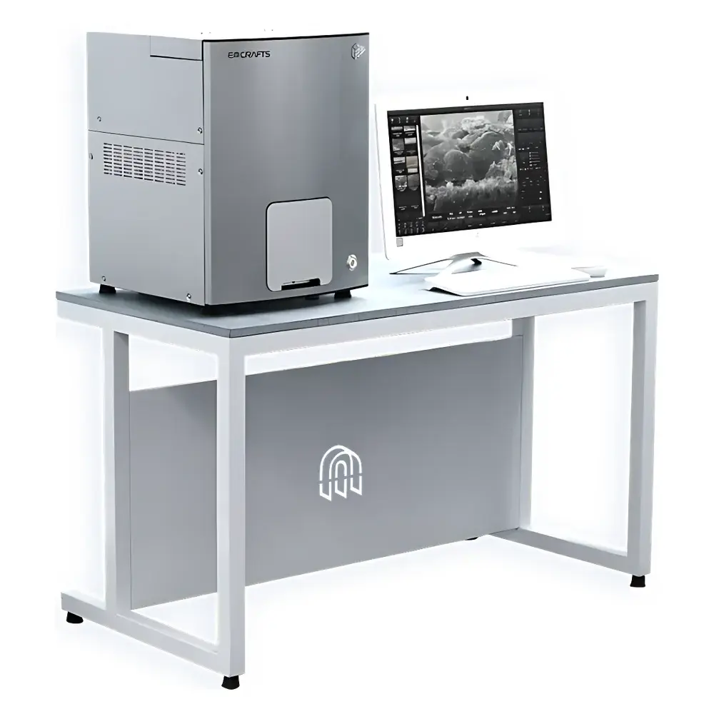
EmCrafts CUBE-II Desktop Scanning Electron Microscope
| Brand | EmCrafts |
|---|---|
| Origin | Guangdong, China |
| Manufacturer Type | Authorized Distributor |
| Product Category | Domestic |
| Model | CUBE-II |
| Price Range | USD 140,000–210,000 |
| Instrument Type | Benchtop SEM |
| Electron Source | Tungsten Filament |
| Secondary Electron (SE) Resolution | 1.0 nm at 30 kV |
| Magnification Range | 100× to 800,000× |
| Accelerating Voltage | 0.5–30 kV |
| Backscattered Electron (BSE) Resolution | 4.0 nm at 30 kV |
| Maximum Sample Dimensions | Ø80 mm × H53 mm |
| Stage Motion | X/Y: ±21 mm (42 mm travel), Z: 5–43 mm (38 mm travel), Tilt: –90° to +90° (manual), Rotation: 360° (motorized) |
| Standard Detectors | In-lens Secondary Electron Detector (SED), Solid-State Backscattered Electron Detector (BSED) |
Overview
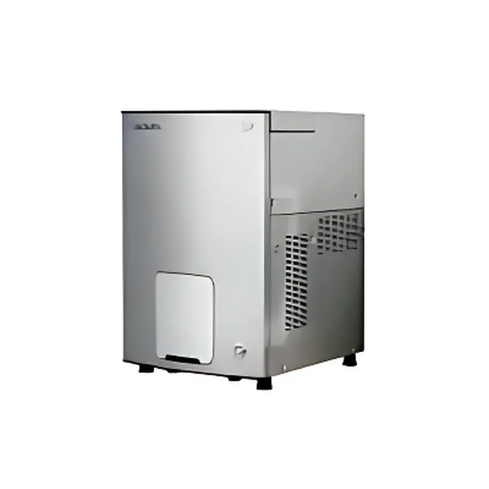
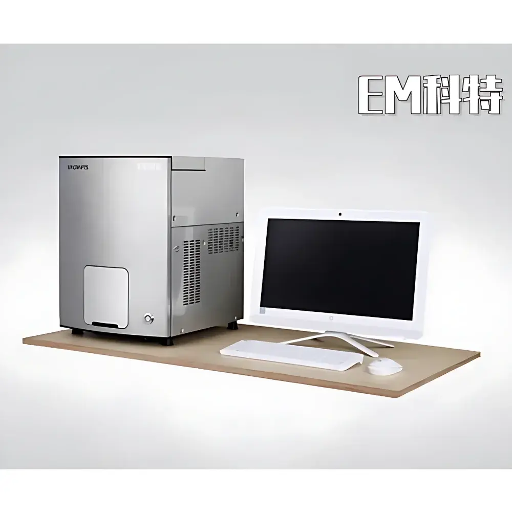
The EmCrafts CUBE-II is a high-performance benchtop scanning electron microscope (SEM) engineered for laboratories requiring nanoscale imaging capability without the infrastructure demands of conventional floor-standing systems. Utilizing thermionic emission from a tungsten filament electron source and optimized electromagnetic lens optics, the CUBE-II delivers true SEM contrast mechanisms—including topographic (SE), compositional (BSE), and edge-enhanced signals—within a compact, self-shielded chassis. Its operational principle relies on raster-scanning a focused electron beam across conductive or metallized samples while collecting emitted secondary and backscattered electrons to reconstruct high-fidelity grayscale micrographs. Designed for rapid deployment, the system achieves vacuum readiness in ≤90 seconds and venting in ≤10 seconds via an integrated turbomolecular pump and pressure-regulated airlock—eliminating dependency on dedicated HVAC or reinforced flooring. The CUBE-II meets fundamental requirements for materials characterization in academic research, quality control labs, and failure analysis workflows where space, budget, and workflow agility are constrained.
Key Features
- Sub-2 nm secondary electron resolution at 30 kV, enabling visualization of fine surface topography including grain boundaries, nanoparticle morphology, and fracture features.
- Integrated 5-axis motorized stage with coaxial geometry: X/Y translation (±21 mm), Z-height adjustment (5–43 mm), continuous 360° rotation, and manual tilt (–90° to +90°)—critical for multi-angle imaging and stereo reconstruction.
- Self-contained vacuum architecture with dual-stage pumping: scroll pre-pump and 200 L/s turbomolecular pump, achieving base pressure <5 × 10⁻⁵ Pa in under 90 s.
- No electron gun alignment required during routine operation; factory-aligned tungsten filament cartridge ensures long-term beam stability and reproducibility.
- Modular detector configuration: standard in-lens SE detector for high signal-to-noise topographic imaging and solid-state BSE detector for atomic number contrast, both optimized for low-kV operation down to 0.5 kV.
- Robust high-voltage subsystem rated for continuous operation across 0.5–30 kV, supporting variable landing energy strategies for beam-sensitive or insulating specimens.
Sample Compatibility & Compliance
The CUBE-II accommodates specimens up to 80 mm in diameter and 53 mm in height, compatible with standard SEM stubs (Ø12.7 mm, Ø25 mm, Ø32 mm) and custom holders. Conductive coating (e.g., Au/Pd sputtering) is recommended for non-conductive samples; optional low-vacuum mode (not included) may be added via upgrade kit for hydrated or uncoated biological specimens. The system complies with IEC 61000-6-3 (EMC emissions) and IEC 61000-6-2 (immunity), and its electrical safety conforms to IEC 61010-1 for laboratory equipment. While not certified to ISO/IEC 17025 or GLP as a standalone instrument, the CUBE-II supports audit-ready data acquisition when used with validated software protocols and calibrated reference standards (e.g., NIST-traceable grating samples).
Software & Data Management
Acquisition and analysis are managed through EmCrafts’ proprietary SEM Suite v4.x—a Windows-based application supporting real-time image capture, multi-frame averaging, digital zoom, measurement annotation (line, angle, area, particle count), and export in TIFF, BMP, JPEG, and raw DAT formats. The software implements timestamped metadata embedding (accelerating voltage, working distance, dwell time, detector gain), enabling traceability per ISO/IEC 17025 clause 7.5.2. Optional modules include automated particle analysis (APA), EDS integration interface (for third-party energy-dispersive spectrometers), and remote desktop control via secure RDP over local network. All acquired images retain embedded EXIF-like headers compliant with FAIR data principles (Findable, Accessible, Interoperable, Reusable).
Applications
- Materials science: grain structure analysis of metals/alloys, ceramic porosity assessment, polymer phase separation studies.
- Electronics: solder joint inspection, PCB trace integrity verification, MEMS device metrology.
- Geoscience: mineral identification via BSE contrast, sediment particle morphology classification.
- Life sciences: coated biological tissues, insect exoskeleton ultrastructure, pollen grain surface patterning.
- Forensics & QA/QC: fiber identification, counterfeit component verification, coating thickness estimation via cross-section imaging.
FAQ
Does the CUBE-II require external water cooling or special power conditioning?
No. It operates on standard 100–240 V AC, 50/60 Hz single-phase input with internal air-cooled electronics and no external chiller requirement.
Can the system image non-conductive samples without metal coating?
Standard operation requires conductive coating for optimal SE imaging. Low-vacuum or variable-pressure modes are available as optional hardware upgrades.
Is the stage fully motorized, including tilt?
X, Y, Z, and rotation axes are motorized; tilt is manually controlled via precision knurled knob with angular scale markings.
What vacuum level is maintained during imaging?
Operating chamber pressure is typically 1–5 × 10⁻⁴ Pa during routine SE/BSE imaging at 5–30 kV.
How is calibration verified for quantitative measurements?
Calibration is performed using certified NIST SRM 2090 (line grating) or similar traceable standards; users can execute daily drift checks via stage repeatability routines built into SEM Suite.