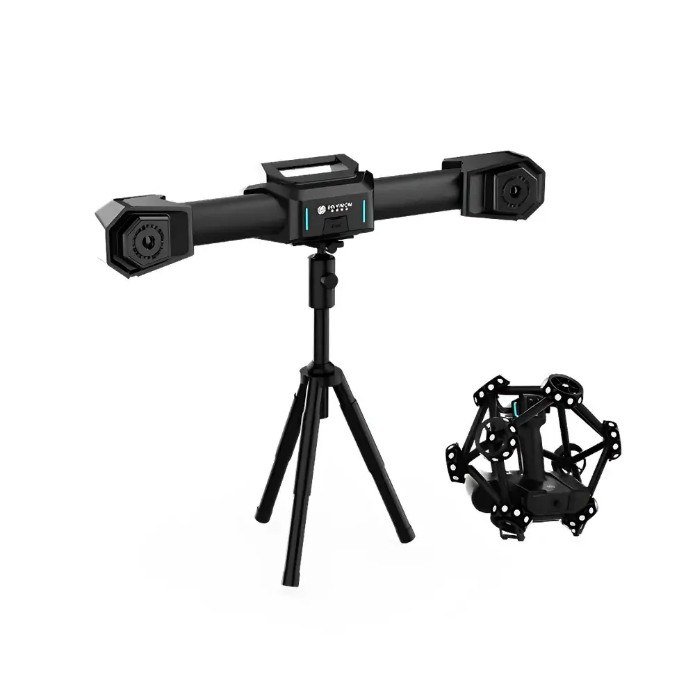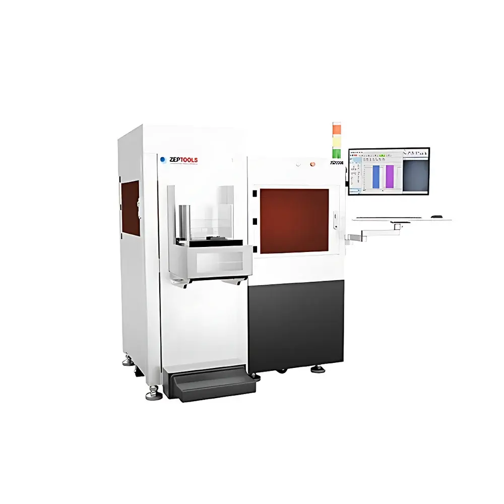
ZEPTOOLS JS2000B Automated Stylus Profilometer
| Brand | ZEPTOOLS |
|---|---|
| Origin | Anhui, China |
| Manufacturer Type | Authorized Distributor |
| Country of Origin | China |
| Model | JS2000B |
| Price | Upon Request |
| Positioning Accuracy | Better than ±10 µm |
| Standard Probe Tip Radius | ≥2 µm (60° included angle) |
| Maximum Scan Length | ≤55 mm |
| Step Height Repeatability | ≤0.5 nm |
| Vertical Resolution | 0.05 nm |
| Maximum Sample Size Compatibility | 6-inch and 8-inch wafers |
| Maximum Wafer Thickness | ≤10 mm |
| Wafer Material Compatibility | Silicon, Lithium Tantalate, Glass (opaque, translucent, and transparent) |
| Probe Normal Force Range | 0.5 mg–50 mg |
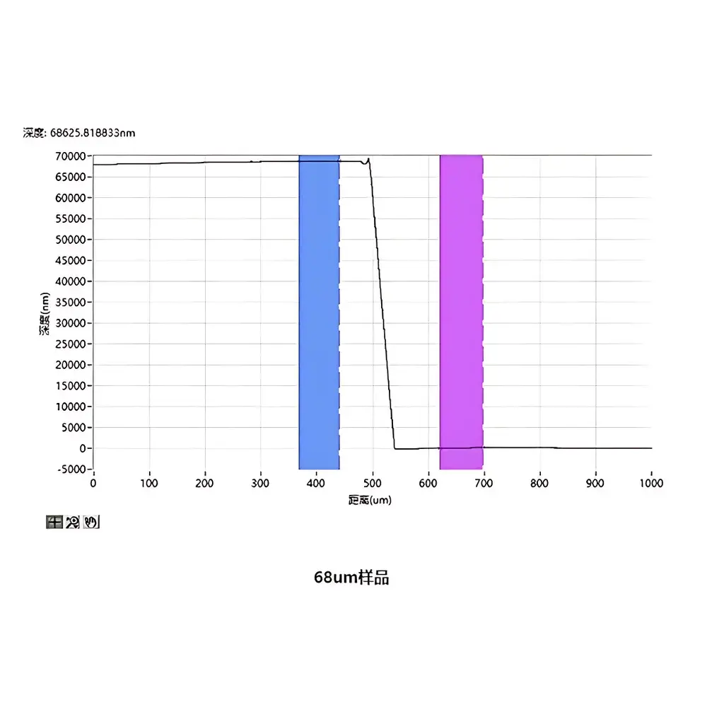
| Maximum Step Height Range | ≤80 µm |
| Image Recognition System Accuracy | Better than ±10 µm |
| Mechanical Stability (Marathon Test) | >500 wafers |
| Throughput | ≥10 WPH (single-side measurement at ≥5 locations) |
Overview
The ZEPTOOLS JS2000B Automated Stylus Profilometer is a high-precision, contact-based surface metrology instrument engineered for nanoscale topographic characterization in R&D and production environments. It operates on the principle of mechanical stylus scanning—where a diamond-tipped probe traverses the sample surface under controlled normal force, converting vertical displacement into high-fidelity analog signals via a differential inductive transducer. These signals are digitized and processed using real-time feedback algorithms to reconstruct 2D cross-sectional profiles and 3D surface maps with sub-nanometer repeatability. Designed specifically for semiconductor process control and advanced materials research, the JS2000B delivers traceable, ISO/IEC 17025-aligned measurements of step height, film thickness, surface roughness (Ra, Rq, Rz), waviness, flatness, warpage, and thin-film stress—without optical interference or assumptions about material optical properties. Its rigid granite base, air-damped isolation platform, and closed-loop Z-axis stage ensure thermal and mechanical stability across extended measurement cycles.
Key Features
- Ultra-low-force probe actuation system (0.5–50 mg range) with active pressure regulation, minimizing surface deformation on soft polymers, photoresists, and low-k dielectrics.
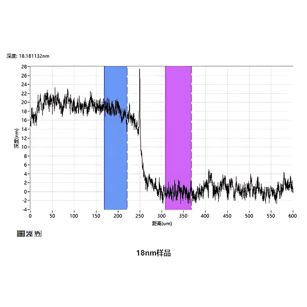
- Sub-angstrom vertical resolution (0.05 nm) and step height repeatability ≤0.5 nm—validated per ISO 25178-6 and ASTM E1558 protocols.
- Integrated coaxial optical imaging system with 10×–50× magnification and real-time probe–sample alignment overlay, enabling feature-specific targeting within ±10 µm positioning accuracy.
- Modular hardware architecture supporting optional FFU (Fan Filter Unit) cleanroom integration, static charge neutralization modules, and SECS/GEM-compliant E84 interface for factory automation.
- One-click multi-point batch measurement workflow for 6″ and 8″ wafers—including automated edge exclusion, center finding, and grid-based scan scheduling.
- Robust mechanical design validated for >500-wafer marathon operation under continuous duty cycle—meeting SEMI S2/S8 safety and reliability benchmarks.
Sample Compatibility & Compliance
The JS2000B accommodates substrates up to 8 inches (200 mm) in diameter and 10 mm thick, including silicon, lithium tantalate, fused silica, quartz, and patterned glass wafers—regardless of optical transparency. Its non-destructive, force-controlled scanning ensures compatibility with fragile MEMS structures, OLED encapsulation layers, and bio-coated surfaces. All measurement outputs comply with ISO 4287 (surface roughness), ISO 25178 (areal surface texture), ASTM F1935 (step height calibration), and USP (pharmaceutical film thickness). Audit-ready data logs include full metadata (operator ID, timestamp, environmental conditions, calibration certificate ID), satisfying GLP and GMP requirements per FDA 21 CFR Part 11 when paired with validated software configuration.
Software & Data Management
The proprietary ZEPTOOLS Profilometry Suite v4.x provides ISO-standardized analysis modules for step height (with multi-point averaging and edge detection), roughness (per ISO 4287/25178), stress calculation (Stoney equation with thermal expansion coefficient input), and 3D surface reconstruction (triangulated mesh export in STL/OBJ formats). Raw data is stored in HDF5 format with embedded calibration parameters and version-controlled processing history. The software supports SECS/GEM communication via E84 interface for integration into AMHS and MES systems. Data export options include CSV, PDF reports with NIST-traceable uncertainty statements, and direct import into JMP, MATLAB, or Python (via open API).
Applications
- Process development and monitoring of etch depth, deposition uniformity, and CMP endpoint detection in front-end semiconductor fabrication.
- Characterization of multilayer stacks in compound semiconductor devices (GaN, SiC), photovoltaic absorber layers, and flexible display TFTs.
- Quantitative evaluation of MEMS mirror flatness, microfluidic channel depth, and medical device coating integrity (e.g., stent polymer layers).
- Failure analysis of delamination, blistering, and interfacial voids through comparative cross-sectional profiling before/after reliability testing.
- Calibration and verification of optical profilers and AFMs using certified step-height reference standards (NIST-traceable SRM 2160/2161).
FAQ
What probe tip specifications are included by default?
The standard probe features a 60° included angle and tip radius ≥2 µm. Optional sub-micron probes (≤1 µm radius, same geometry) are available for high-aspect-ratio trench or sidewall profiling.
Is the system compatible with vacuum or inert gas environments?
The base configuration operates in ambient air; however, the chamber-integrated variant (JS2000B-VAC) supports N₂-purged enclosures and low-vacuum (<10 mbar) operation upon request.
Can the software generate automated pass/fail reports aligned with internal SPC limits?
Yes—the software supports user-defined specification limits per parameter, automatic flagging of out-of-tolerance results, and SPC chart generation (X-bar/R, Cpk) with export to Excel or enterprise QMS platforms.
Does the system meet SEMI standards for wafer handling and factory integration?
It complies with SEMI E10 (definition of equipment reliability), SEMI E11 (equipment communications), and SEMI E84 (SECS/GEM interface), and supports EFEM integration via SMIF pod loading and robotic arm handshaking protocols.
How is traceability maintained for calibration and measurement uncertainty?
Each instrument ships with a factory calibration certificate referencing NIST-traceable step-height standards. Uncertainty budgets follow JCGM 100:2008 (GUM) methodology and are documented in the software’s audit log alongside environmental sensor readings (temperature, humidity, vibration).