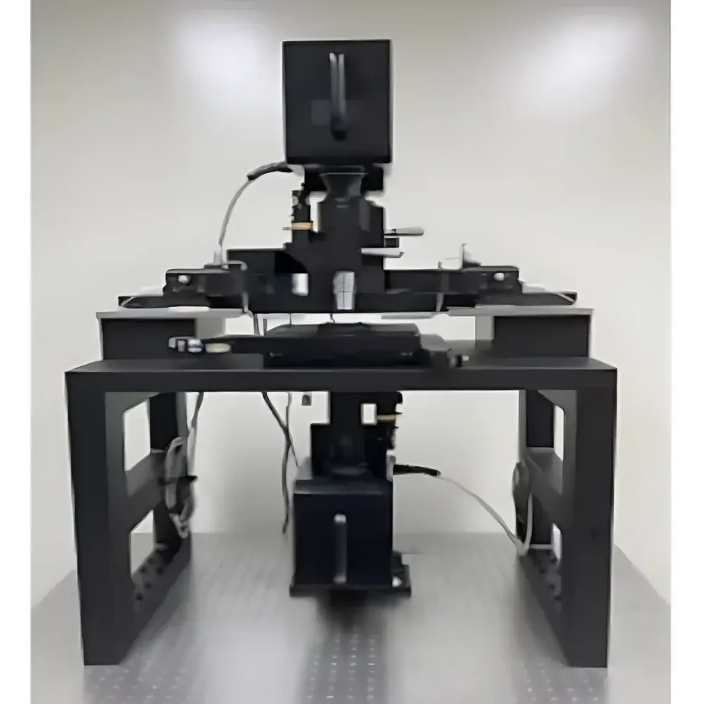
AunionTech M-LED Wafer-Level I-V-L-S Photometric and Spectral Test System
| Brand | AunionTech |
|---|---|
| Origin | Shanghai, China |
| Model | M-LED Wafer Test System |
| Type | Wafer-Level Photometric & Spectral Measurement Platform |
| Key Specifications | Minimum LED size supported: 10 µm |
| Luminance range | 0.0001–10¹⁰ cd/m² |
| Current range | 100 pA – 1 A |
| Measurement outputs | I-V-L curves, chromaticity (CIE x,y), dominant wavelength (DWL), spectral power distribution (SPD), uniformity mapping across LED arrays |
| Configuration | Inverted or upright chip orientation support |
| Platform | Vibration-isolated optical bench with precision XYZ-θ stage |
Overview
The AunionTech M-LED Wafer-Level I-V-L-S Photometric and Spectral Test System is an engineered solution for quantitative, spatially resolved electro-optical characterization of micro-scale light-emitting diodes at the wafer level. Designed specifically for the rapidly evolving Micro-LED and Mini-LED manufacturing ecosystem, this system integrates high-resolution microscopic imaging, programmable probe-based electrical stimulation, and calibrated photometric/spectral detection into a single synchronized platform. Its core measurement principle relies on simultaneous acquisition of current–voltage (I-V) response, luminance (L) via traceable photometry, chromaticity coordinates (CIE 1931 x,y), dominant wavelength (DWL), and full spectral power distribution (SPD) — all under controlled bias conditions. Unlike conventional spot-metering colorimeters, this system performs pixel-level metrology across monolithic or tiled LED arrays, enabling statistical evaluation of parametric yield, spatial non-uniformity, and binning-critical parameters essential for display-grade microdisplay fabrication and AR/VR microdisplay qualification.
Key Features
- Sub-10 µm spatial resolution capability, validated for individual Micro-LED emitters as small as 10 µm × 10 µm — compatible with both flip-chip and upright die configurations.
- Integrated I-V-L-S measurement engine delivering synchronized acquisition of electrical and photometric data, including forward voltage (Vf), leakage current, luminance (cd/m²), CIE chromaticity, dominant wavelength (nm), and normalized SPD (380–780 nm).
- Ultra-wide dynamic range photometry: luminance coverage from 1 × 10⁻⁴ to 1 × 10¹⁰ cd/m²; electrical current measurement spanning 100 pA to 1 A — enabling characterization from sub-threshold leakage to saturated emission regimes.
- Precision motorized XYZ-θ stage with <100 nm repeatability and closed-loop feedback, optimized for automated wafer navigation, die alignment, and multi-point array scanning.
- Vibration-isolated optical platform compliant with ISO 10360-2 mechanical stability requirements, minimizing drift-induced uncertainty during long-duration spectral integration.
- Modular probe station architecture supporting customizable DC/pulsed bias configurations, thermal chuck options (−40 °C to +150 °C), and optional environmental enclosures for humidity-controlled testing.
Sample Compatibility & Compliance
The system supports bare wafers (2″, 4″, 6″, 8″) and processed LED-on-sapphire, LED-on-Si, or hybrid bonded substrates. It accommodates standard probe card footprints and enables direct contact probing without die singulation. All photometric calibrations are traceable to NIM (National Institute of Metrology, China) standards, with spectral responsivity certified per CIE Publication 127:2007 and luminance linearity verified per CIE TN 005:2021. The platform satisfies functional requirements for GLP-compliant R&D environments and provides audit-ready metadata logging required for internal quality systems aligned with ISO/IEC 17025:2017 clause 7.8. Data export formats include CSV, HDF5, and XML—structured to facilitate downstream integration with MES or SPC platforms.
Software & Data Management
Control and analysis are performed via AunionTech’s proprietary WaferScan Pro software suite, built on a deterministic real-time acquisition kernel. The interface supports scriptable test sequences (Python API), multi-parameter correlation analysis (e.g., Vf vs. DWL shift), and automated uniformity reporting per die or sub-array region. All measurements embed timestamp, stage position, environmental sensor readings (temperature, humidity), and instrument calibration IDs. Audit trails comply with FDA 21 CFR Part 11 requirements for electronic records and signatures, including user authentication, change history, and immutable raw-data archiving. Exported datasets include embedded metadata conforming to ASTM E2913-20 (Standard Practice for Digital Image Data Exchange).
Applications
- Parametric yield analysis during Micro-LED epitaxial development and process optimization.
- Pre-bonding wafer-level screening for display backplane integration (e.g., CMOS-driven RGB microdisplays).
- Quantitative assessment of emission uniformity across large-area tiled arrays for AR waveguide illumination systems.
- Correlation studies between structural defects (observed via integrated dark-field microscopy) and localized electroluminescent anomalies.
- Reliability stress testing (DC/AC/pulsed) with in-situ photometric degradation tracking.
- Support for JEDEC JESD253A (Micro-LED Display Reliability Test Method) and draft ISO/IEC AWI 5159 (Micro-LED measurement terminology and methods).
FAQ
What wafer sizes does the system support?
Standard configurations accommodate 2-inch through 8-inch wafers; custom stages are available for 12-inch substrates upon request.
Is spectral calibration traceable to national standards?
Yes — spectral irradiance and luminance calibrations are traceable to NIM (China) with documented uncertainty budgets per ISO/IEC 17025.
Can the system perform pulsed I-V-L-S measurements?
Yes — the source-measure unit supports pulse widths from 10 µs to continuous DC, with synchronization to spectrometer integration gates.
Does the software support automated binning based on CIE chromaticity tolerances?
Yes — users define Δu’v’ or MacAdam ellipse limits; the system generates pass/fail maps and exports bin assignment tables compatible with industry-standard sorting protocols.
Is remote operation and monitoring supported?
The system includes secure TLS-encrypted web-based remote access for status monitoring, job queue management, and diagnostic telemetry — compliant with IEC 62443-3-3 cybersecurity requirements for industrial control systems.