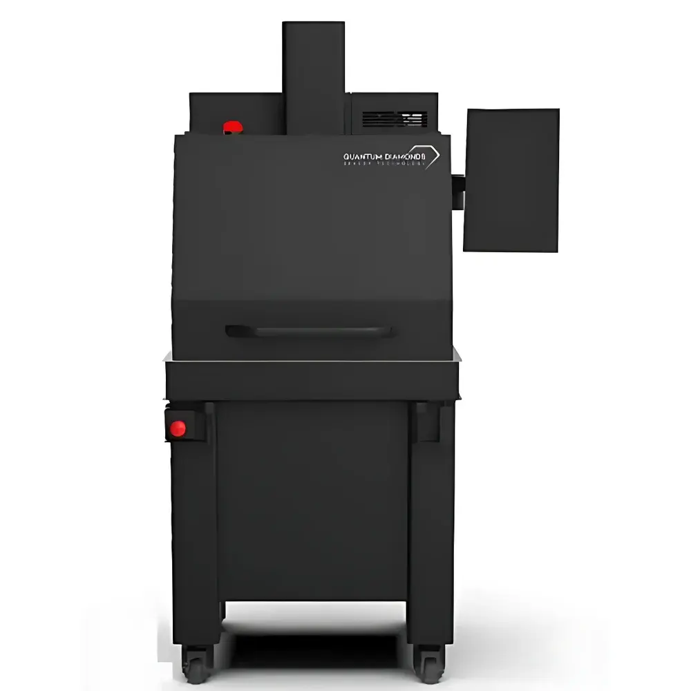
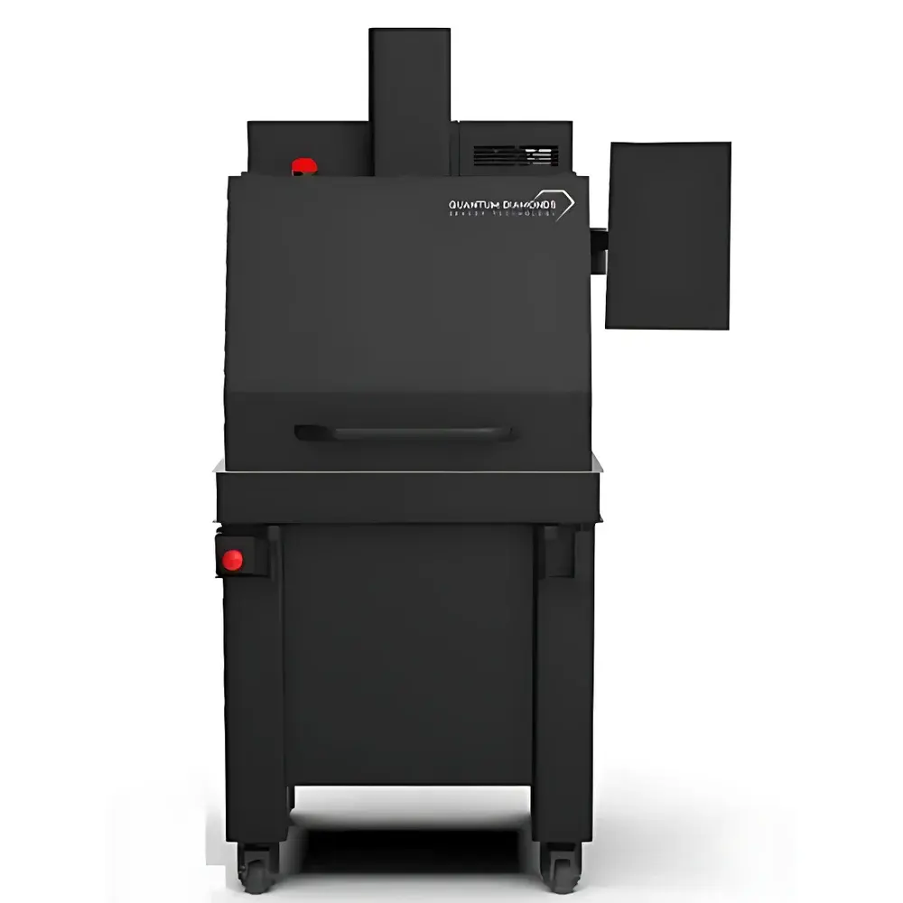
Auniontech 3D Magnetic Current Imaging Microscope (Quantum-Enhanced Super-Resolution Microscope)
| Brand | Auniontech |
|---|---|
| Origin | Shanghai, China |
| Manufacturer Type | Authorized Distributor |
| Product Category | Domestic |
| Model | 3D Magnetic Current Imaging Microscope |
| Price | Upon Request |
Overview
The Auniontech 3D Magnetic Current Imaging Microscope is a quantum-enhanced super-resolution instrument engineered for non-invasive, quantitative current mapping in complex heterogeneous integrated circuits and advanced packaging structures. Unlike conventional optical or electron-based microscopy techniques, this system operates on the physical principle of high-sensitivity magnetic field detection—leveraging optically pumped magnetometers (OPMs) or quantum diamond nitrogen-vacancy (NV) center sensors to resolve nanoscale current distributions with three-dimensional spatial fidelity. It enables direct visualization of active current paths through silicon, interposers, and multi-layer redistribution layers without destructive cross-sectioning. Designed specifically for failure analysis (FA) labs in semiconductor R&D and high-reliability manufacturing, the microscope delivers sub-micrometer depth localization and sub-200 nm lateral resolution under ambient laboratory conditions—eliminating the need for cryogenic cooling, vacuum environments, or ion-beam sample preparation.
Key Features
- True 3D current reconstruction: Simultaneous imaging of current flow across multiple stacked metallization layers (e.g., TSVs, microbumps, RDLs) with axial separation down to 85 µm
- Non-destructive magnetic current imaging (MCI): Penetrates CMOS passivation and packaging materials without signal attenuation—de-capping only required
- High-fidelity vector field mapping: Measures both magnitude and direction of magnetic flux density (Bz) with DC–4 GHz bandwidth and <1 nT/√Hz AC sensitivity
- Wide-field capability: 4 mm × 4 mm field-of-view enables full-die current profiling without stitching artifacts
- Robust room-temperature operation: Air-cooled architecture; no liquid helium, lasers, or ultra-high vacuum systems required
- Automated layer decomposition: Proprietary QD software applies physics-constrained inverse modeling and supervised machine learning to isolate layer-specific current densities from raw B-field data
Sample Compatibility & Compliance
The system accommodates standard IC packages—including flip-chip, 2.5D/3D stacked dies, fan-out wafer-level packages (FOWLP), and chiplet-based assemblies—up to 300 mm × 300 mm in footprint. Sample mounting uses vacuum chucking with XYZ translation (300 mm × 300 mm × 20 mm travel range), supporting both bare die and packaged units. The measurement methodology complies with industry-standard failure analysis workflows outlined in JEDEC JESD22-A108 (electrostatic discharge stress testing) and IPC-9701A (current-induced failure mechanisms). While not certified for GLP/GMP production release, the system supports audit-ready data provenance via timestamped metadata logging, operator ID tagging, and exportable raw sensor files compatible with ASTM E2912-22 (standard guide for electromagnetic emission characterization).
Software & Data Management
The QD Analysis Suite provides an integrated environment for acquisition, reconstruction, and interpretation. Core modules include: (1) Real-time magnetic field acquisition with configurable averaging and spectral gating; (2) Layer-wise current inversion using finite-element method (FEM)-based forward modeling coupled with L1-regularized optimization; (3) Comparative overlay tools enabling side-by-side correlation with CAD layout files (GDSII/OASIS import); (4) Batch processing pipeline compliant with FA lab SOPs, including automatic report generation (PDF/HTML) with embedded traceability fields. All processed datasets retain full raw sensor metadata (timestamps, temperature logs, coil calibration coefficients) to satisfy FDA 21 CFR Part 11 requirements for electronic records in regulated development environments.
Applications
- Identification and localization of latent shorts, resistive opens, and electromigration-induced voids in advanced nodes (≤7 nm FinFET, GAA transistors)
- Thermal-current coupling analysis during dynamic power cycling (e.g., DVFS transitions, burst-mode operation)
- Validation of EM simulation models against empirical current distribution maps
- Failure root cause analysis in automotive-grade SoCs and AI accelerators subjected to AEC-Q100 stress profiles
- Current uniformity assessment across heterogeneous integration interfaces (e.g., Si-to-Si, Si-to-GaN bonding)
FAQ
What types of samples can be imaged without de-capping?
Only fully encapsulated packages require de-capping; bare dies, wafer-level test structures, and open-cavity packages are compatible as-is.
Is the system compatible with automated FA workflows?
Yes—API access (Python/C++ SDK) enables integration with SEM-based probing stations and automated test equipment (ATE) for closed-loop fault isolation.
Does the system support time-resolved current imaging?
Yes—AC mode supports phase-resolved current mapping at frequencies up to 4 GHz, with temporal resolution limited by sensor bandwidth and signal averaging settings.
How is calibration traceability maintained?
Each system ships with NIST-traceable magnetic field reference sources and factory calibration certificates; in-house recalibration is performed using Helmholtz coils and calibrated fluxgate standards.
Can the microscope distinguish between eddy currents and conduction currents?
Yes—the combination of DC/AC sensitivity modes, frequency-domain filtering, and vector field modeling allows separation of displacement-related eddy effects from primary conduction paths.